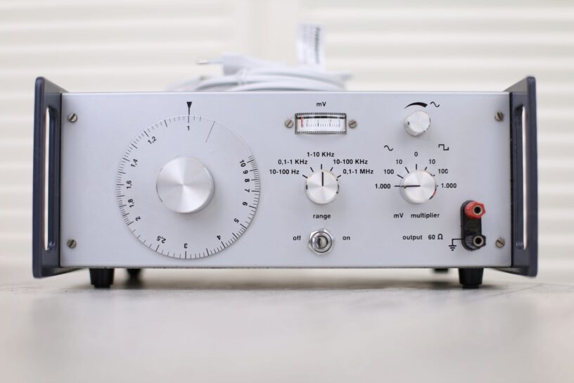
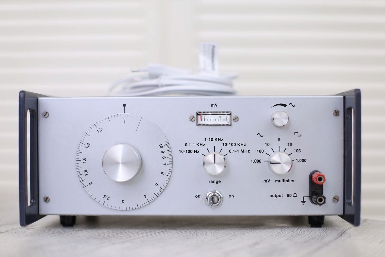
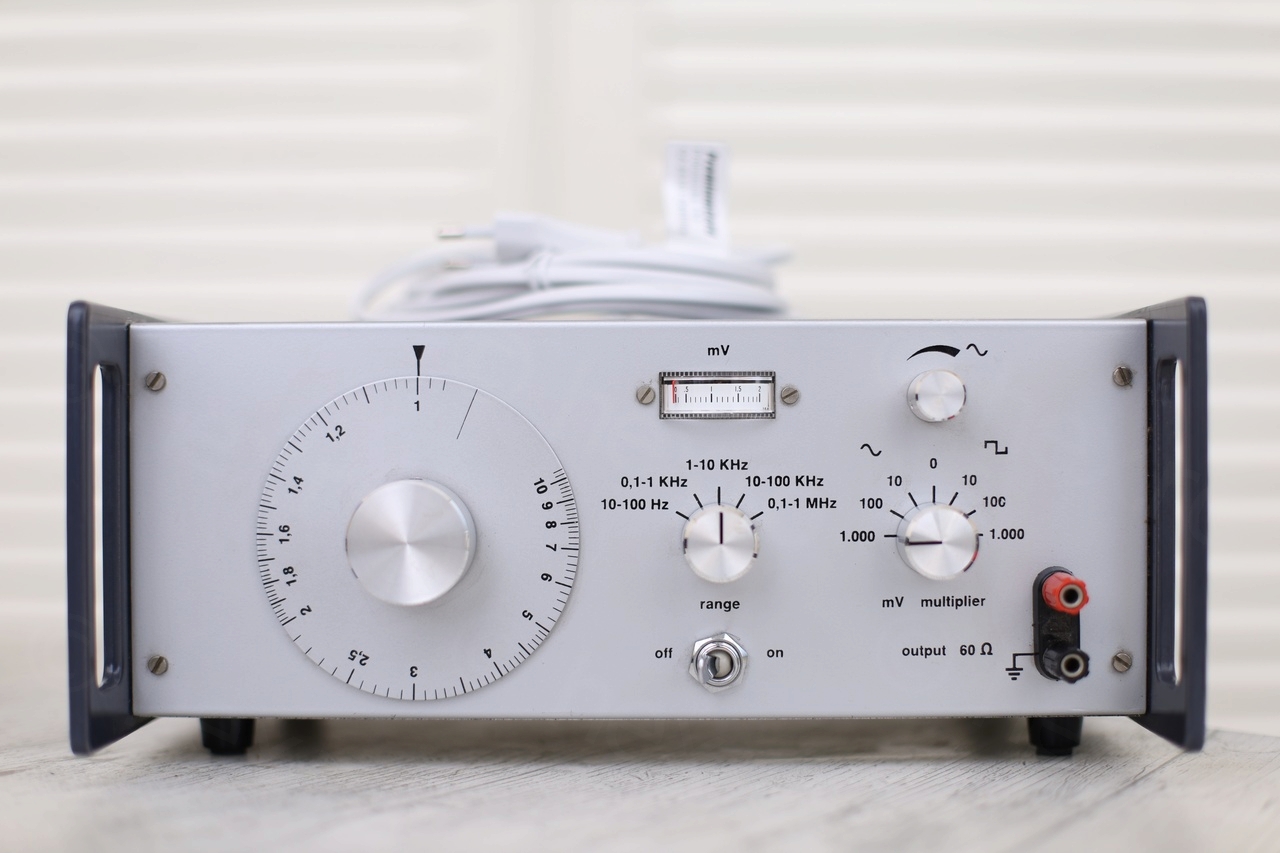
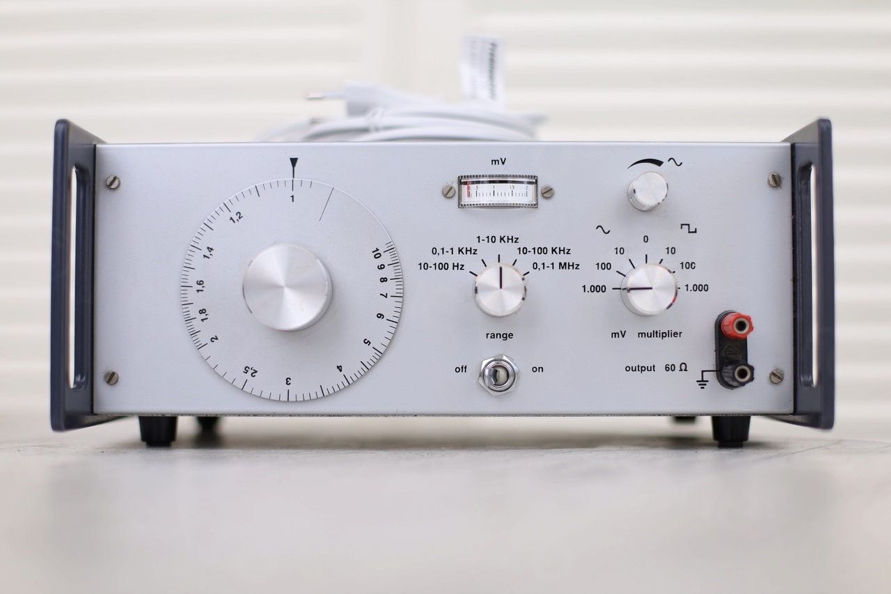
I saw this device at the local flea market and it was intriguing. It lacked any description, but it looked factory made – nice Aluminum finishing, professional buttons / labels. Since some of the screws were missing and I could see a large variable capacitor inside, I figured the price is right if just for the capacitor itself.
Table of Contents
- Exterior Aspect
- Interior aspect
- But what is this thing ?!
- “État des lieux”
- Component layout
- T3 Transistor – Source terminal Voltage problem
- T7 Transistor – Incorrect Base voltage
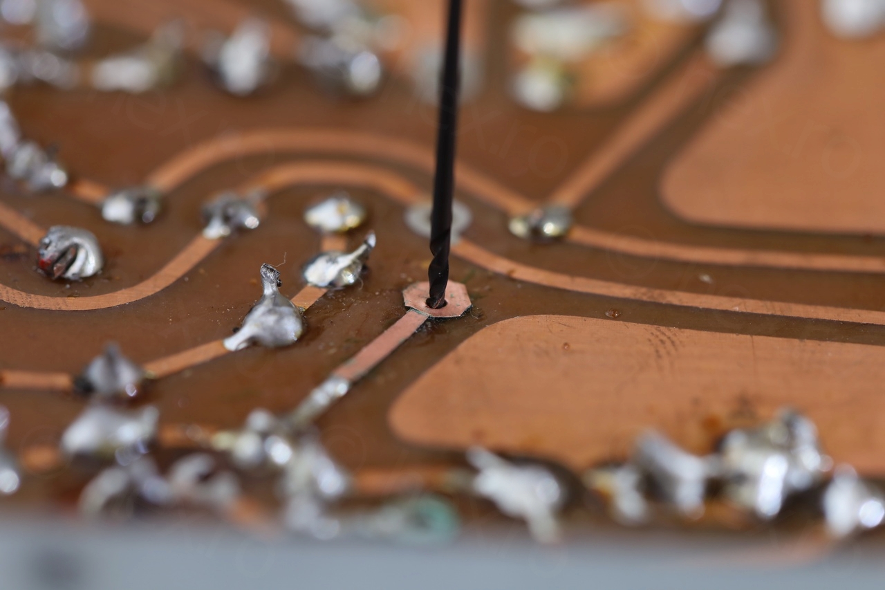
- Lifted traces replacement, cleanup
- Final tests
Exterior Aspect

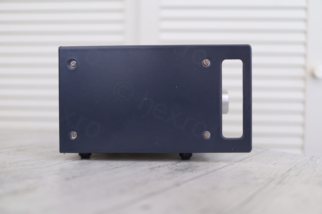
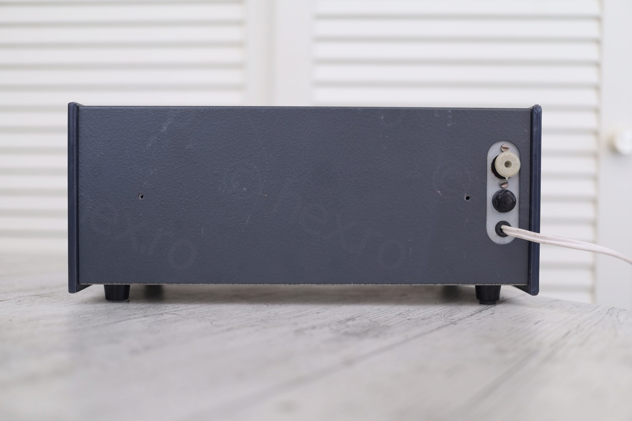

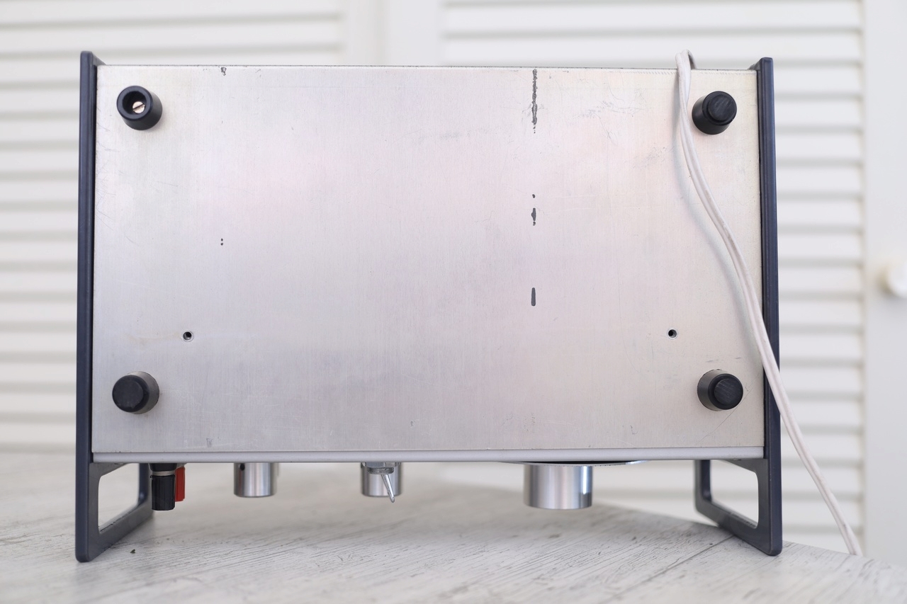
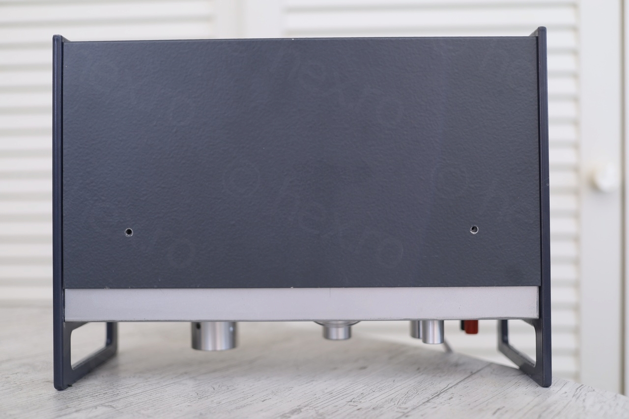
The device looked clean – except the top / bottom screws that were missing but more importantly it was the lack of any marking / model. Who made this thing ?
Interior aspect
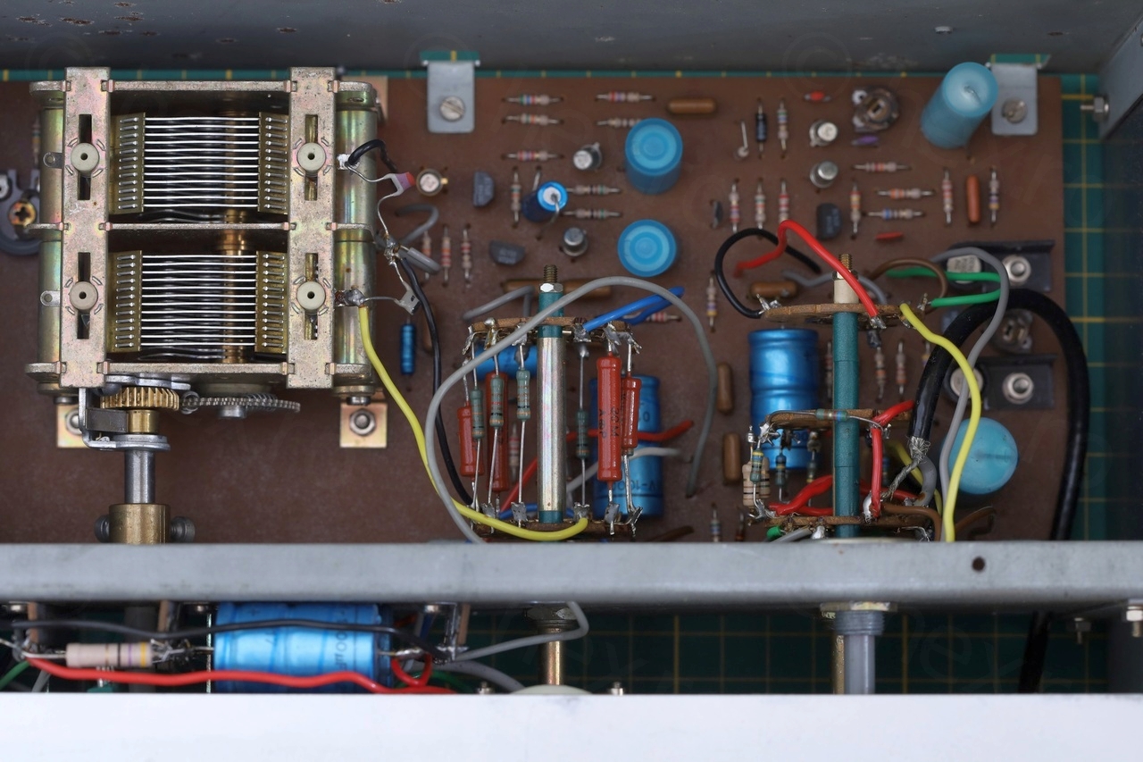

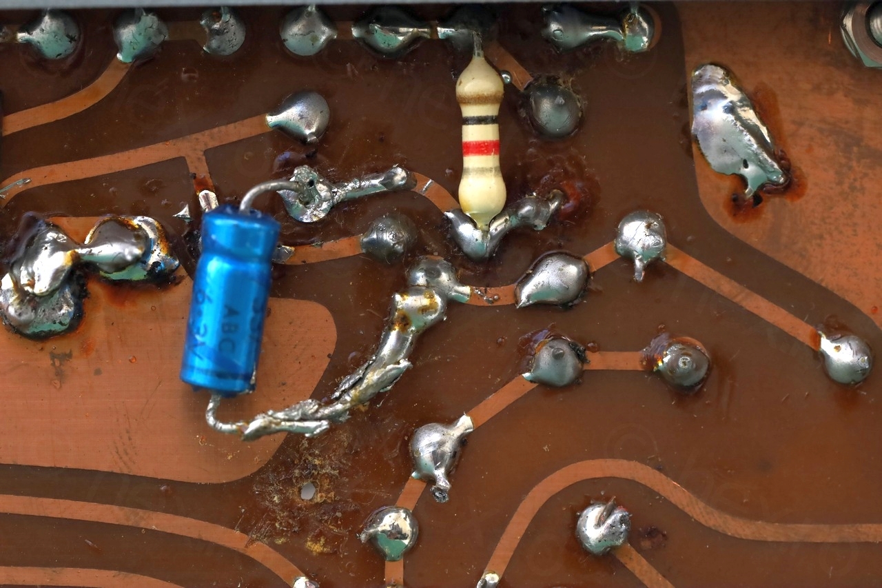
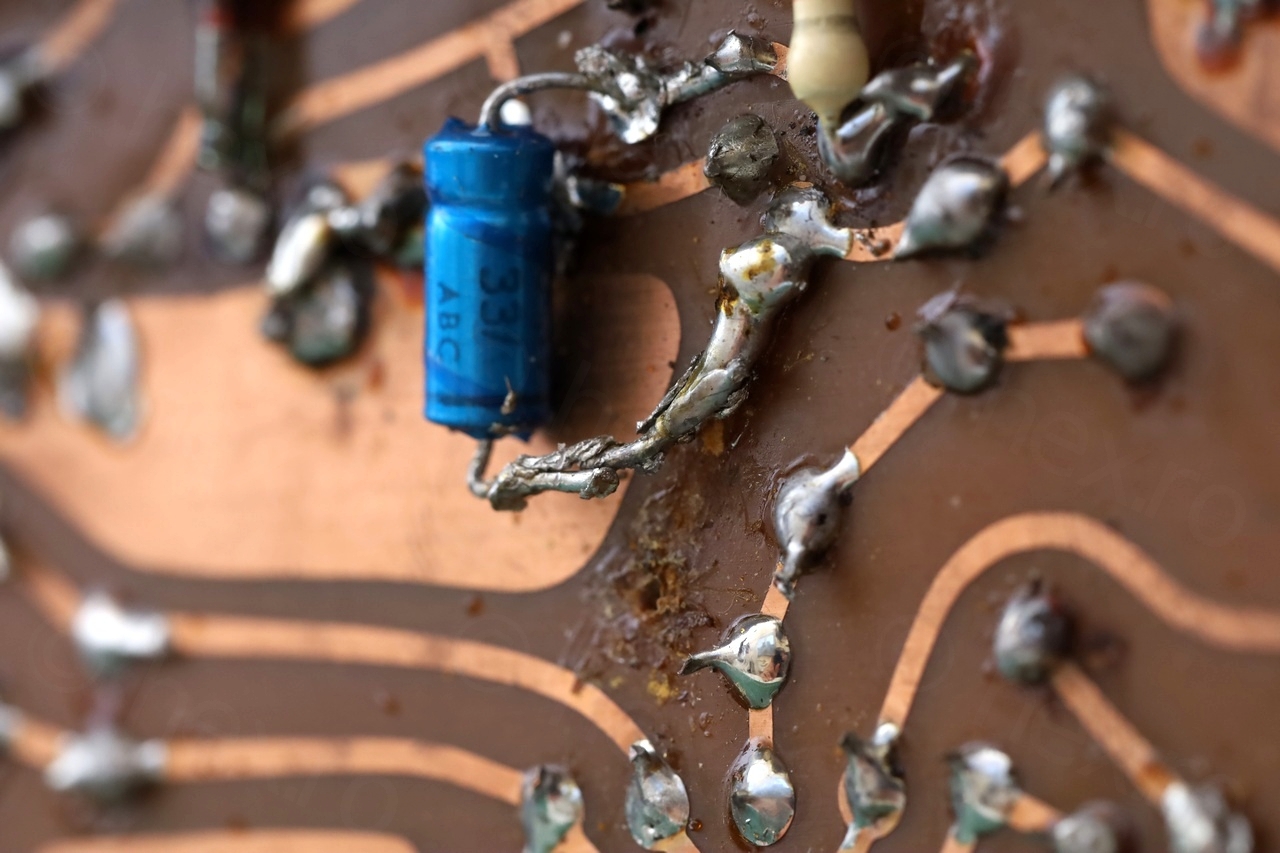

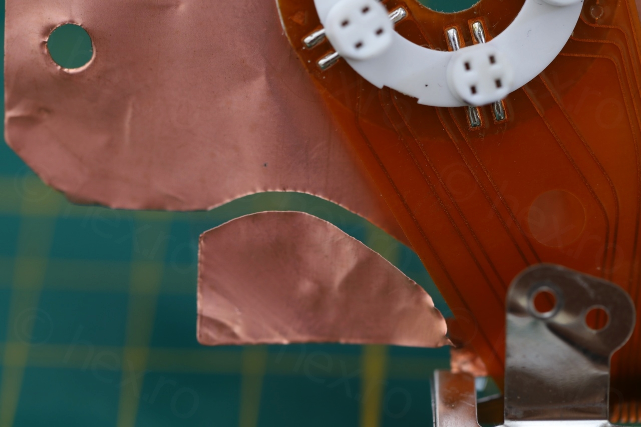
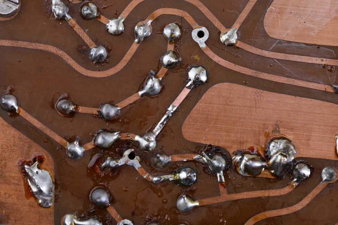
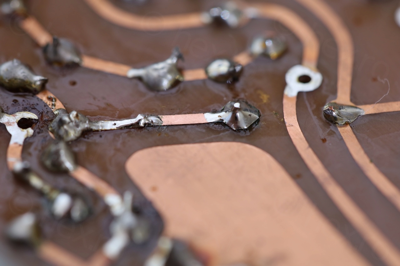
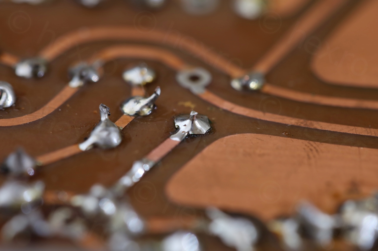
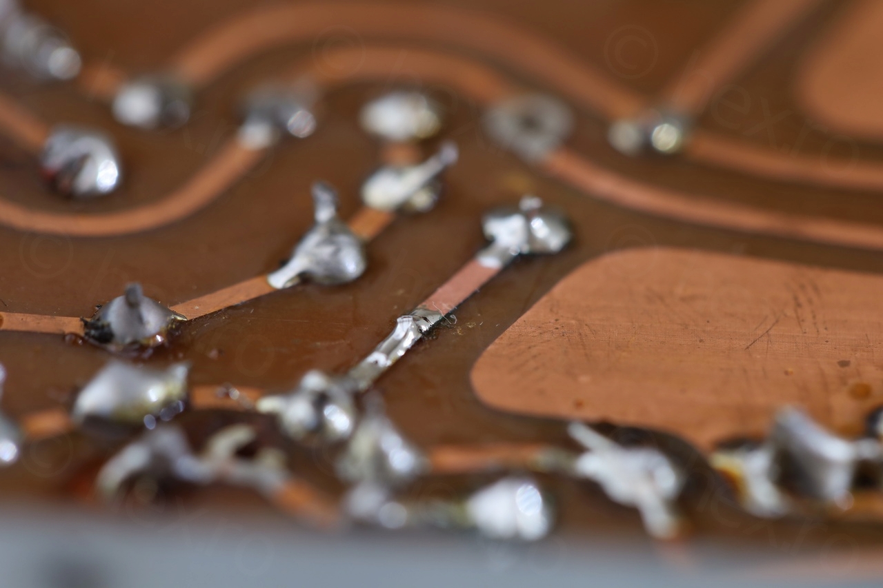
The interior hand a stark contrast to the exterior. The large solder joints look cold, as made with a not powerful enough iron. Instead of the solder flowing properly, it looked like smaller blobs melted over smaller blobs. Some traces were lifted, and some components cut from the main side of the board and soldered on the back.
It looked more and more like it was an assembled kit – the owner made an error when assembling it – and it was easier to try to salvage the situation by soldering on the back on the circuit board.
But what is this thing ?!
Capacitor was still tempting, it was also tempting to try to repair / salvage the device. But what was it ? I kept searching Google – but “tone generator” or “audio generator” or “signal generator” were returning too many results. I decided to use one of the output transistors as criteria, and, after many searches, what do I spot at the END of the search results ?
It is a Philips BEM-014 Tone Generator!
Now with a name – it was easy to find a schematic.
There are two schematics that I was able to find. One that is sharp (I assume the initial one). The second one contains few pages more – including the calibration procedure, that somebody seems to have inserted into the original schematic. The insert operation affected the quality of the existing pages though.
“État des lieux”
I still kept wondering weather I should just salvage the capacitor and dispose of the rest. Curiosity won though and I powered it on to see if it still works.
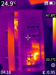
Upon powering on – the good news was that the device did not blow up – nor any capacitors. I took some temperature readings after letting it on for a while.
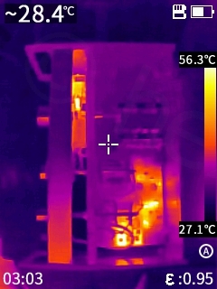
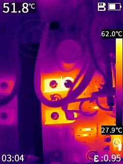
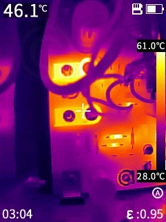
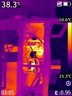
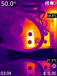
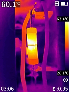
The puzzling thing about the temperatures was that one output transistor was way hotter than the one nearby.
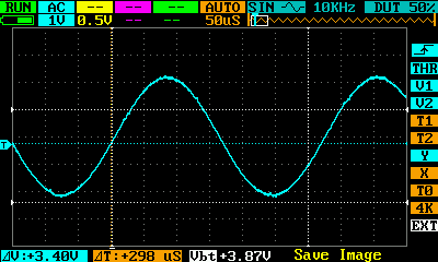
Having a look at the output waveform – it was also problematic. It looked good as the device was powered on, but 2 minutes into the operation it started clipping:
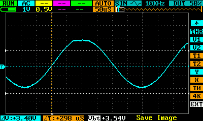
Pffff. Thus it wasn’t anymore about lifted traces and moving the components back to their original place – but also, figuring out what is wrong with it.
In the following video it can be seen that the output settles down to a nice sinusoidal, but it starts clipping stronger and stronger as time goes by:
Component layout
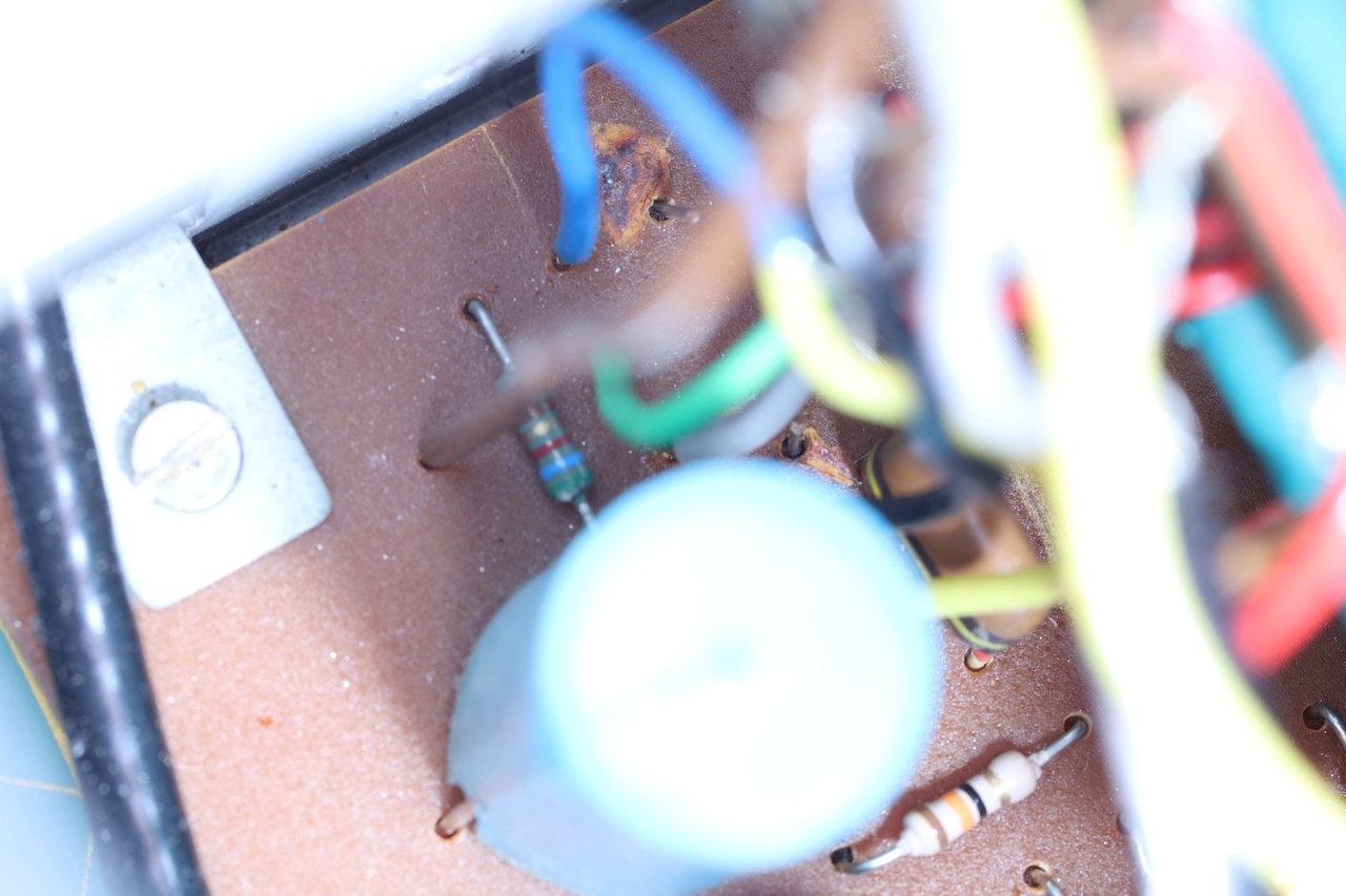
The available schematic / service manual does show the voltages and they are readable. However, the scan of the component layout is very poor and only half of the component identifiers are readable. I had to spend some time to identify the components based on their connections on the board itself and in the schematic:
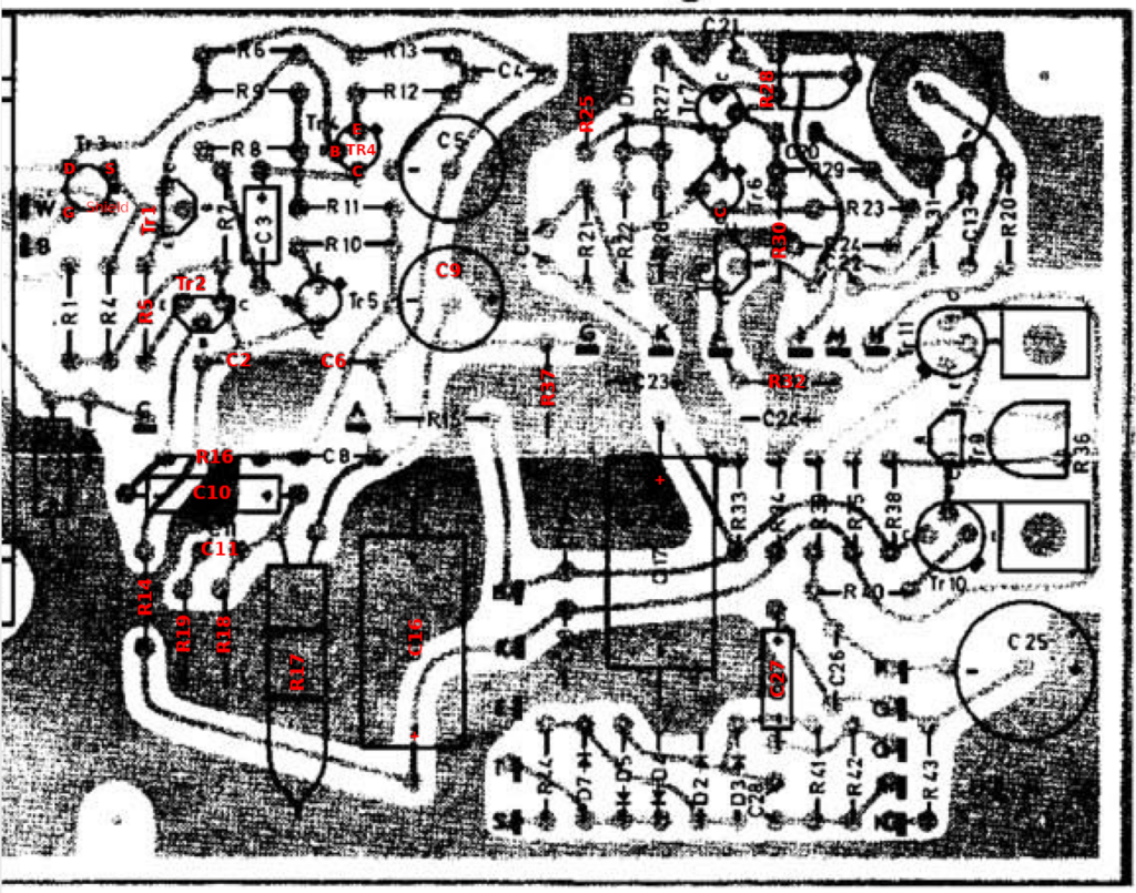
This was needed so that I can find my way around faster, when measuring the voltages, since … I decided I’d like to salvage the device.
T3 Transistor – Source terminal Voltage problem
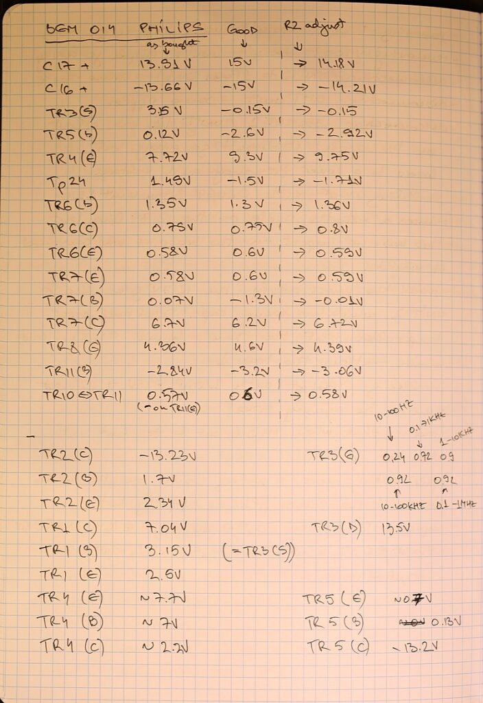
Made a table of the “as bought” / “good” voltages, where the “good” column represents the voltages indicated in the schematics, while “as bought” are the voltages from the device.
Trouble was that many of the voltages were wrong, including the ones on the FET transistor T3 (BFW61). And since the whole circuit seems to be a big feedback loop, I had a hard time figure out what would cause such a big shift. Not de-soldering any parts at least. After looking for a while and knowing that somebody tried to fix some damage on the board, I spotted that the R2 potentiometer was turned all the way towards the big capacitor. But pots should be somewhere in the middle, otherwise what is the point of having an adjusting potentiometer, if the “correct” position is one of the extremes ?
So I decided to move the potentiometer to its center position. And Bingo.
All voltages fell into place. This is the column “R2 adjust” in the table above. I started writing the new voltages down, and when I reached the TR7 (Base), my heart sank. It was supposed to be -1.3V, but I was only measuring 0V …
T7 Transistor – Incorrect Base voltage
By this time I was almost loosing hope. The circuit was still a big feedback loop, and while the damage was very localized now (only the Base voltage of TR7 (BSY39) was off) still hard for me to say where this comes from. Its base should have been at -1.3V but something was not keeping it down, and was 0.
The way I found the problem was by using psychology instead of electrical troubleshooting. I was set on somebody having assembled the device from a kit. And an idea came to mind, did they actually use the correct value resistors ?
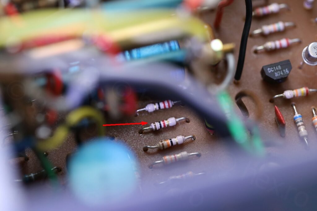
And I found the culprit. I could not believe first, thus I triple checked. R34 is connected to the negative rail, but instead of being 22Ω, a 1kΩ resistor was present instead. Thankfully, I had 22Ω (0.5W) already – even if a tad smaller than the existing ones, it should just still feel original.
Lifted traces replacement, cleanup
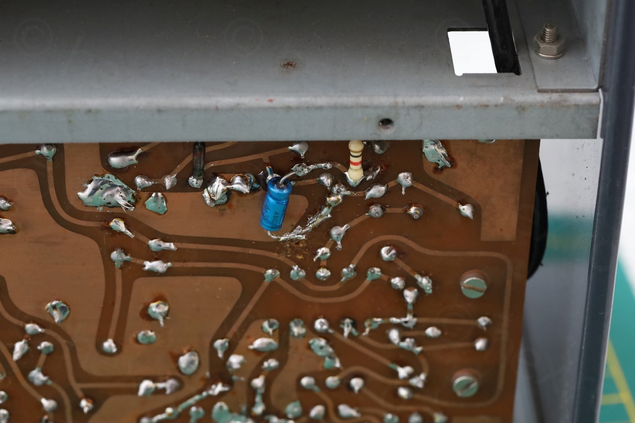
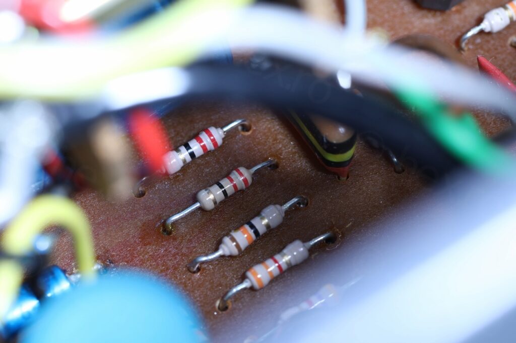
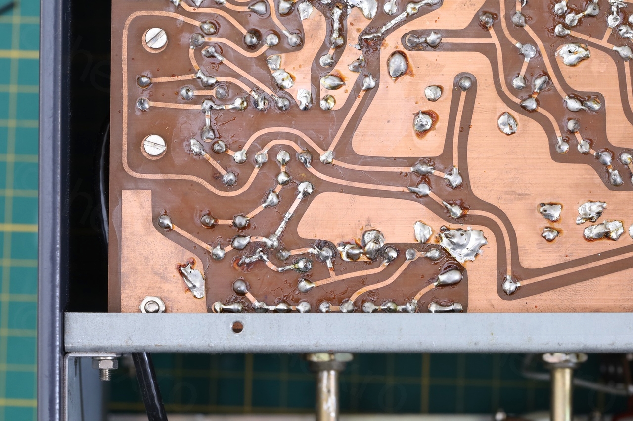
Now with the circuit working and voltages correct, the last thing to do was to clean up the improvisations made in the previous repair / installation attempt.
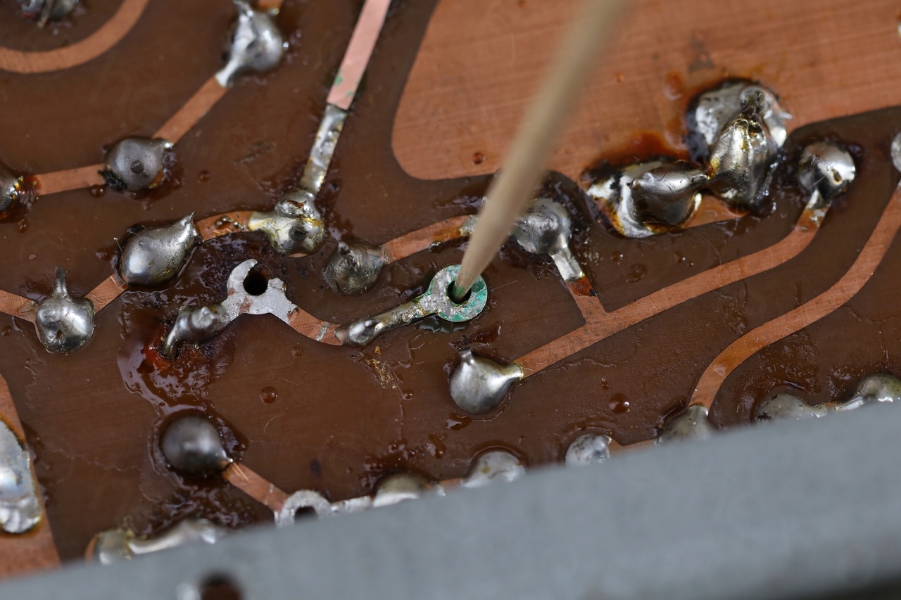
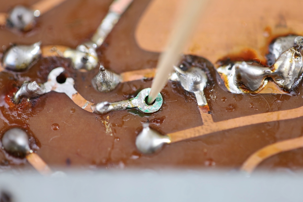
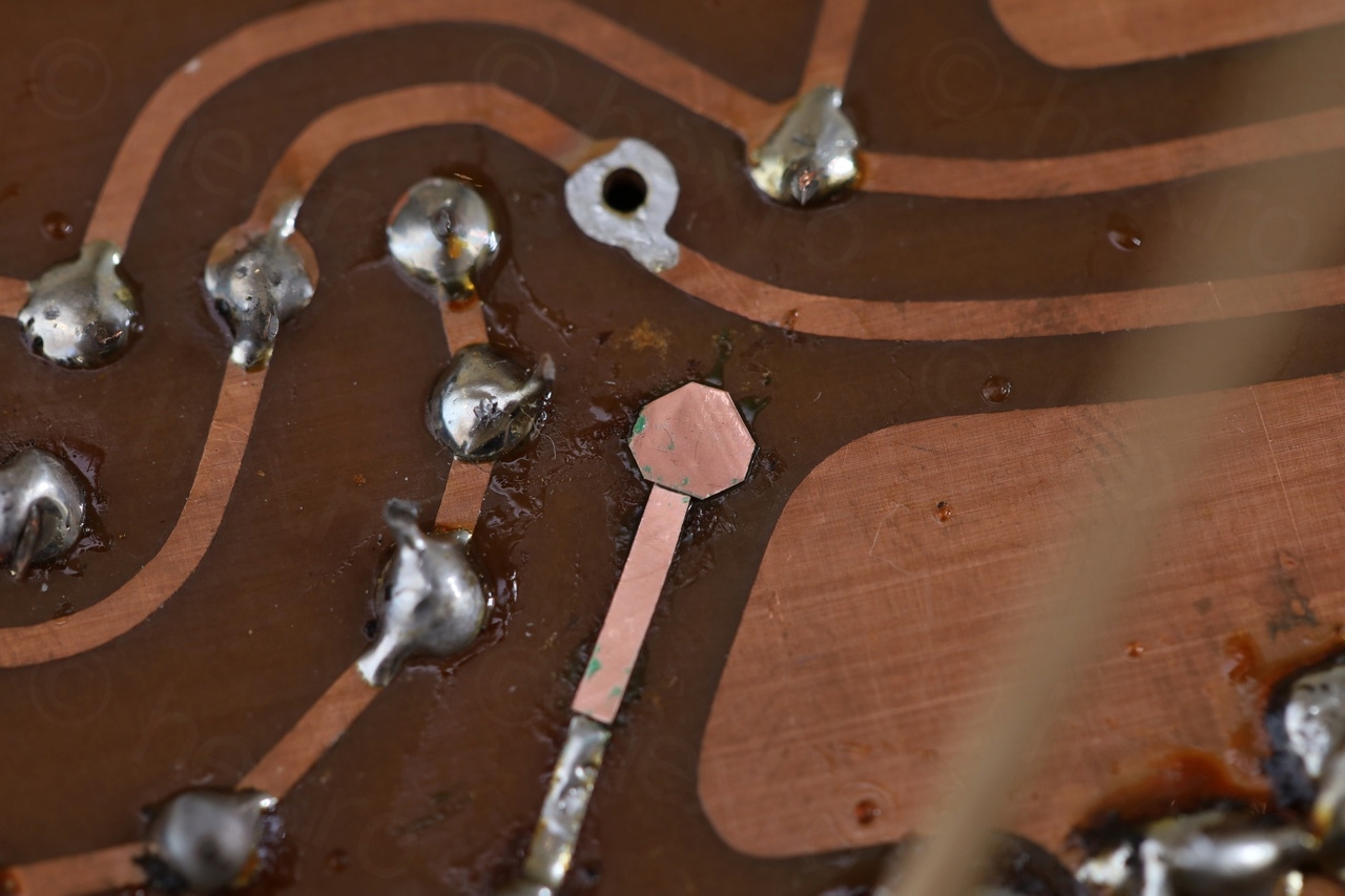
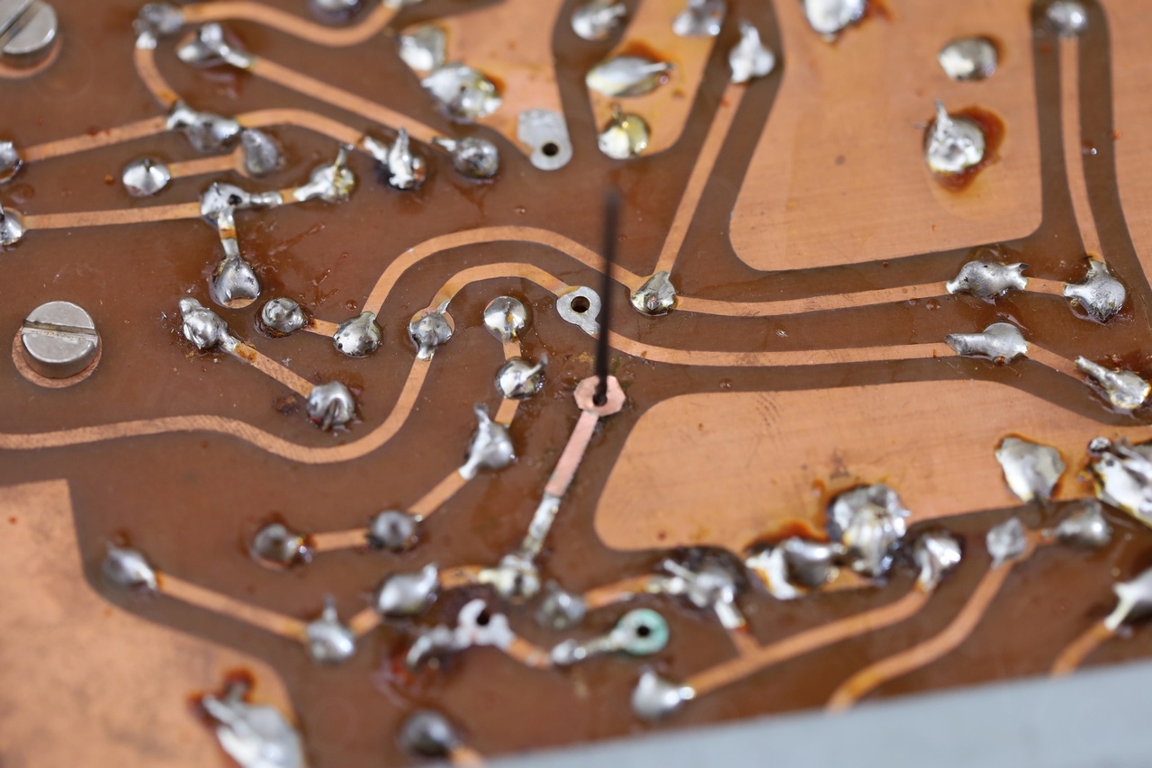
I had to rebuild one missing trace, glue back down another lifted one and move the components back to the component side of the board.


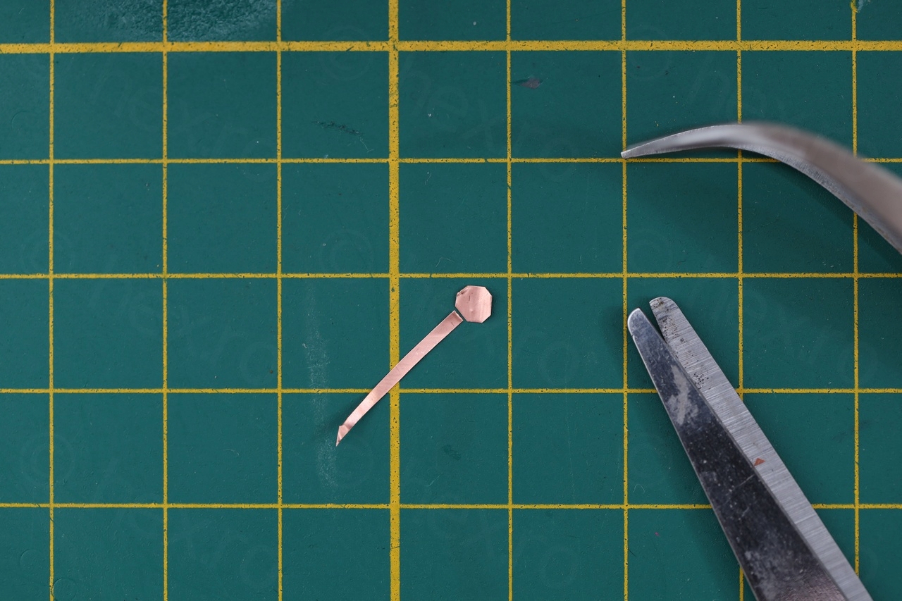
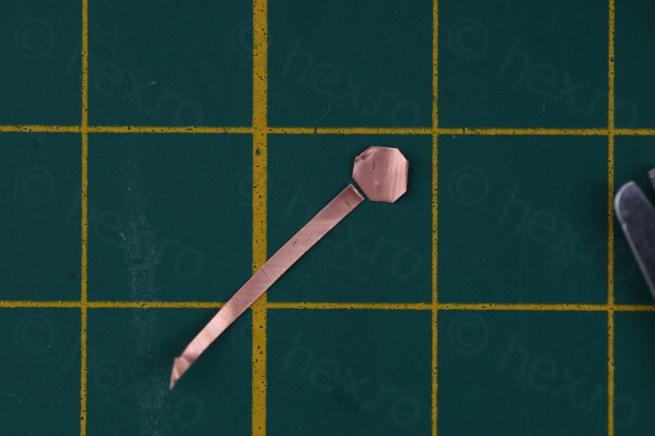
To rebuild the missing trace, I used a salvaged part from a video camera – which was a thin sheet of copper material. I cut it to size:
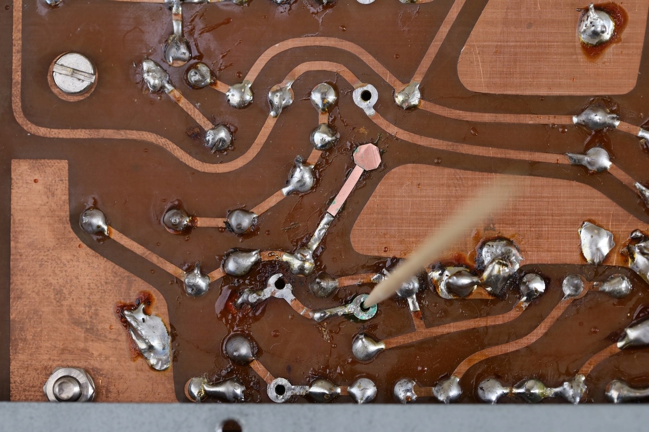
Then I have arranged it on the board after having applied CW2500 epoxy from Circuitworks underneath the trace (used as undercoat instead of over coat). The toothpick was used to keep the other trace pinned down as the epoxy was curing.


Then I have installed all the parts back onto the circuit board. It was rather tricky to access without having it dismantled – which is probably what made the previous repair attempt look so bad. I mean the attempt was working, why do people contend with only minimum-minimorum ?
Due to the small size of the islet – I did not drill the hole before, but after the epoxy has hardened. This way the islet was completely glued and not deformed.

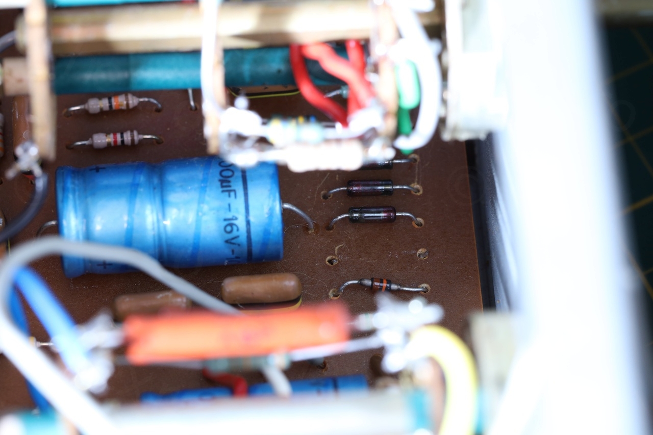
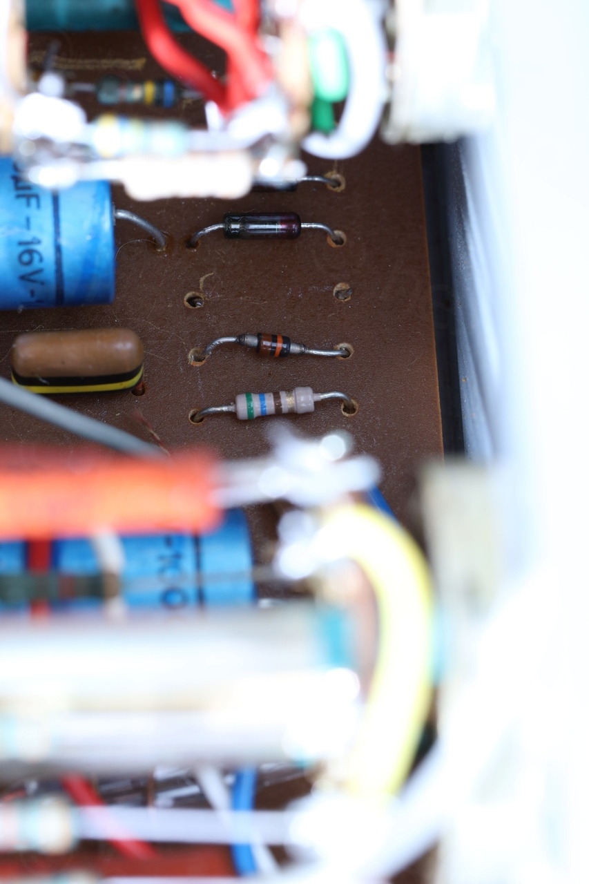
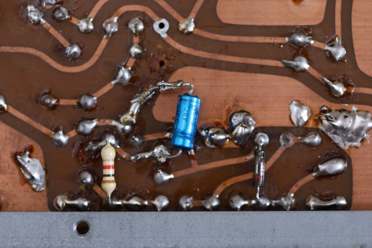
Two photos with the diode and the capacitors on the correct side of the board:

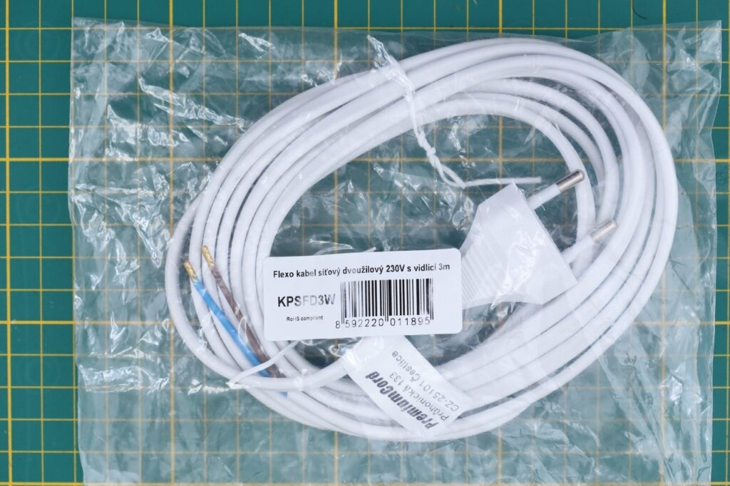
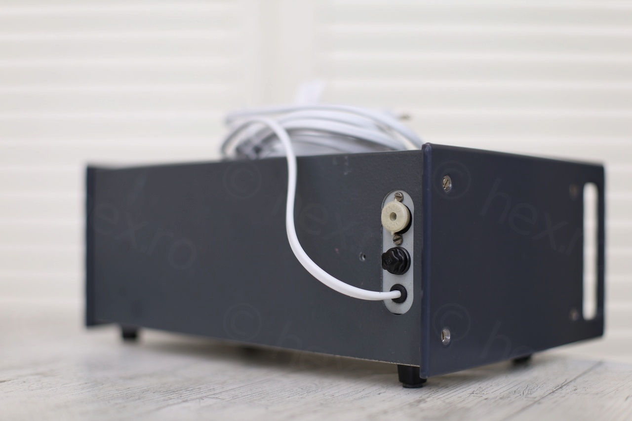
I decided to also replace the power chord, since the initial one felt flimsy:
Final tests
I went trough one more round of testing to make sure that the right voltages produce the right output.
The Sinusoidal output is perfect:
Unfortunately, the square output is not centered on Ground, the lower level of the output even sits above Ground:
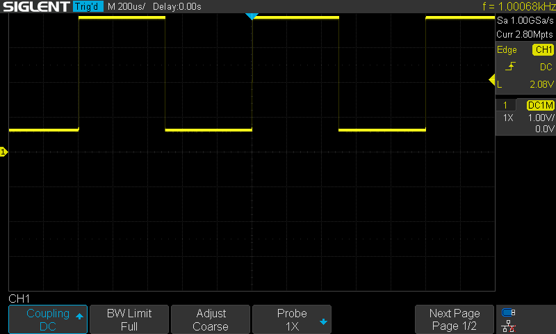
Since voltages were all correct now, I decided to not pursue the checks to see if the square wave output was meant to be like this, or if there was something else wrong with the device.
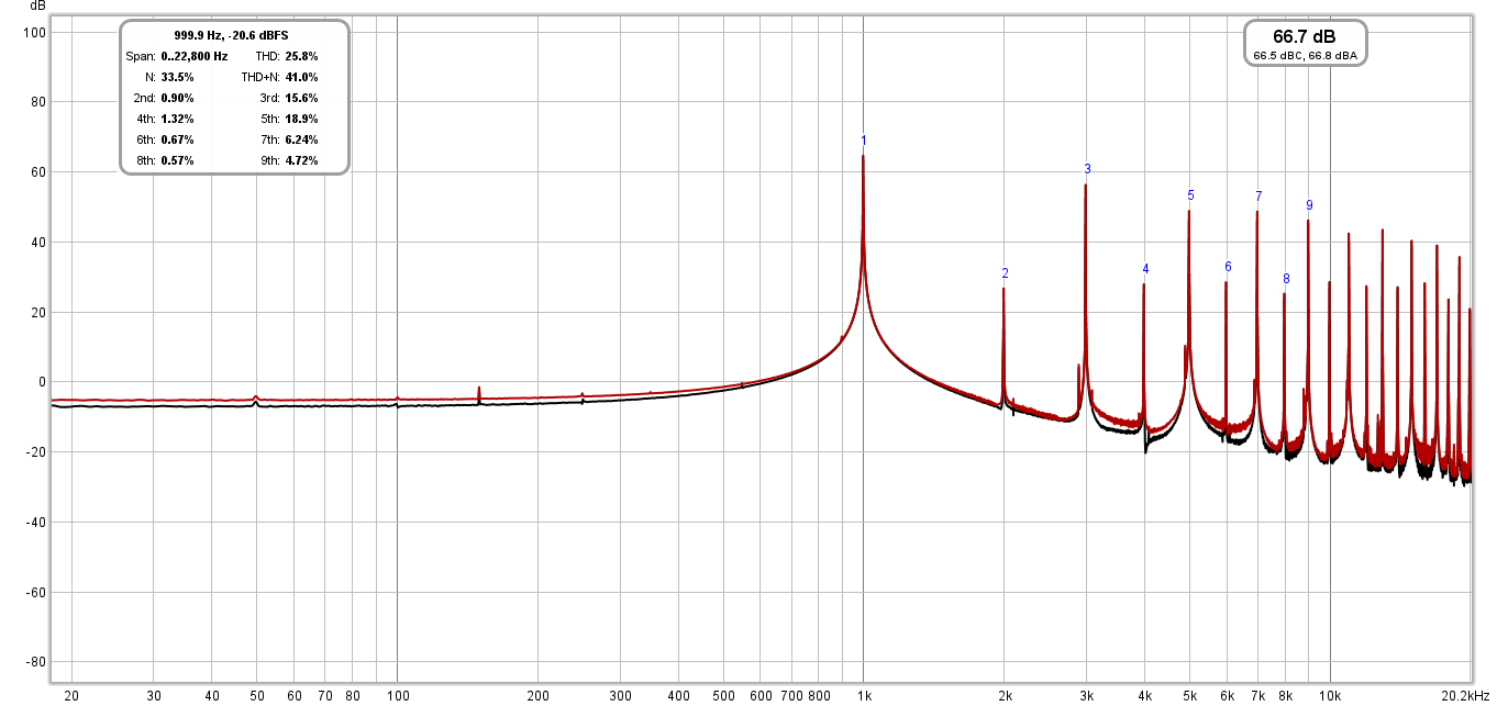
The service manual mentions that the THD is less than 0.1% so I decided to test this too at least at 1kHz – and indeed, is a little less than 0.1%!

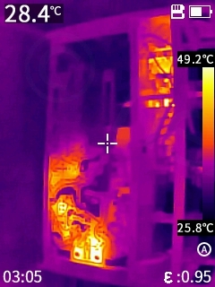
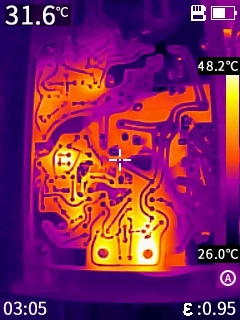
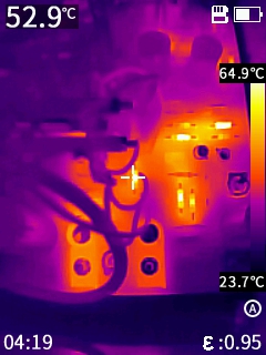
Temperatures also equalized on the output transistors:
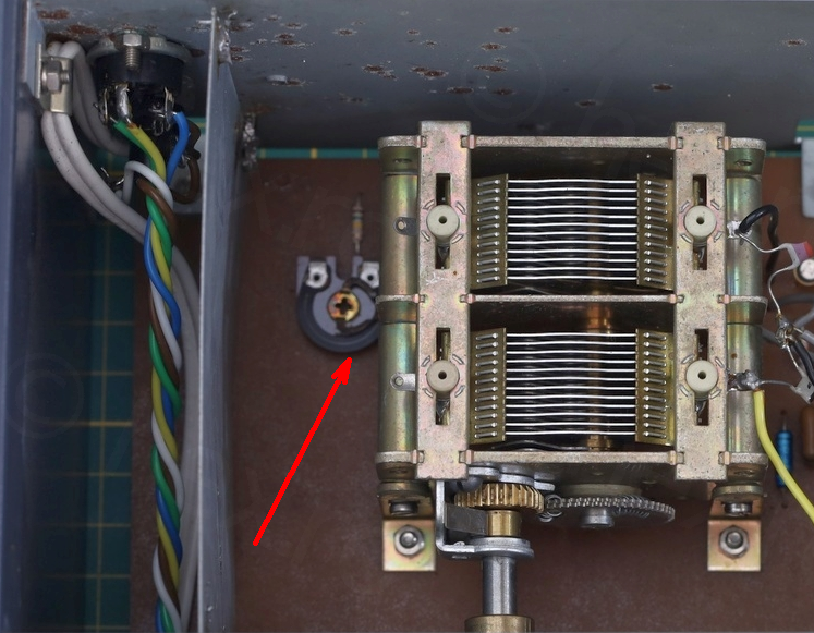
The problem with the device is that it doesn’t seem to cover the whole range. If I make it so that it start at 1kHz and trying to turn it all the way through, I can only rotate it to 9kHz position and then I can’t rotate it anymore. The physical limit is imposed by the variable capacitor, it already traveled all the way through to its opposite end.
I measured the high value resistances and they are within tolerances. I don’t know if this can be improved. Since I would probably not use it on a day to day basis (probably keep it as a donor for a 500pF variable capacitor) I decided not to pursue it. The AWG I have is much more flexible, and even it takes long to boot, it has two outputs and more flexibility in the configuring the wave output.
Finally, some photos after I found some spare screws around to at least attach the case properly to the chassis:
Pieter de Jong
Hello,
I recently bought one of these. I read your article with interest!
I’m trying to get more into repairing older equipment but i also would not mind if this one worked immediately, i need another signal generator.
I did not yet dare to switch it on (the fuse was blown) so I did a preliminary inspection. It looks quite ok except for a tiny resistor that seems to be rather burned. It still is very close to the correct resistance from the schematics but I cannot read the markings itself anymore due to the damage. But i still think i should replace it, perhaps it is not the right resistor. So I looked at the schematic and i found it (R64) but now comes the embarrassing thing: the schematic says 50(ohm)2 and i don’t know what the 2 after the Ohm sign means. Is it Watts? does it mean 52 Ohm? If it’s two watts then the resistor next to it is supposed to be 5 Watts, isn’t that a bit excessive? Anyway I hope someone knows these schematics better than me. Thanks in advance for your advice!
viulian
Hello,
Thank you for the interest in the article!
50Ω2 means 50.2Ω
Unit in the middle is a placeholder for decimal separator. For example, 3k3 means 3.3kΩ. I believe it is because on real paper schematics where fonts are small, the dot (decimal separator) could be easily missed ?
Good luck with your unit!
PS: If I recall right, most resistors were 0.5W – but there are size charts online to help you figure it out.
Pieter de Jong
Thanks! I see it now. I have little experience with these higher precision resistors and did not recognize it. Values like 3k3 I understand but this was new to me. I bought a new resistor so i can replace the baked one and continue testing the device. (also a few fuses hehe)
Pieter de Jong
Hi, small update: i have it working now. Looking at the scope the frequencies are pretty close to the dial so good enough for the amplifiers and guitar pedals I’m working on r.n. The square wave seems to show the same behaviour as your unit, always above ground. As I’m from the Netherlands the manual was not that hard to read, it says:
“Square wave: 3 fixed voltages: 4V, 400mV and 40mV (peak to peak at zero load)
These voltages correspond with the following levels: 0,8V to 4,8V / 80mV to 480mV/ 8mV to 48mV.
The square wave is superimposed on a DC of 0,8V / 80mV or 8mV which could be easily removed by a suitable condenser (sic) ”
Thanks again!
viulian
Congratulations 🙂
I am thankful for the translations related to the square waves, at least it clarifies the situation. I thought something else might have been wrong, but at least now I know.
Best of luck with your projects!
Henk D
Thnx for sharing your experiences with this nice LF generator.
If the full 1:10 frequency range is not obtained, the capacitance of C30 / 31 connected in parallel to the var. capacitor has to be reduced. The ratio of these caps is also important since the amplitude flatness over the range 1:10 is determined by this ratio. If the ratio is set correctly the flatness is in the order of 1mV for 1V output over the full range.
Pls. note that compared to an awg, the distortion figures of this generator are an order of magnitude better. Besides, it can be improved further by a factor 3-4 by replacing the source resistor R4 of the FET with a current source of 0.7mA. After this modification, measurements with a Keithley 2015THD dmm showed a distortion of less than 0.02% in the range 100 – 20kHz.