
Table of Contents
- Overview
- Battery leakage / cleanup
- DIY External Battery Pack
- Populating the External Cache memory sockets
- Benchmarks
- Booting the PC
Overview
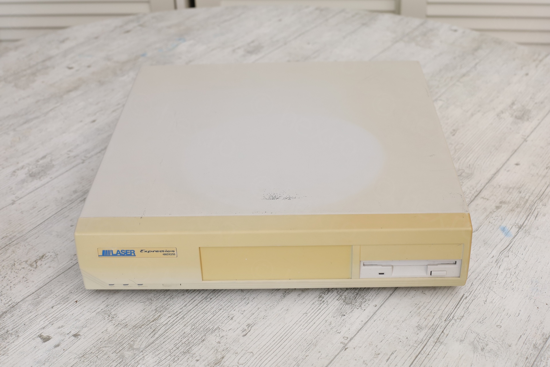
I bought this computer at a Museum sale. While there were plenty systems to pick from, this was sleek – pizza box form factor – and caught my eye.
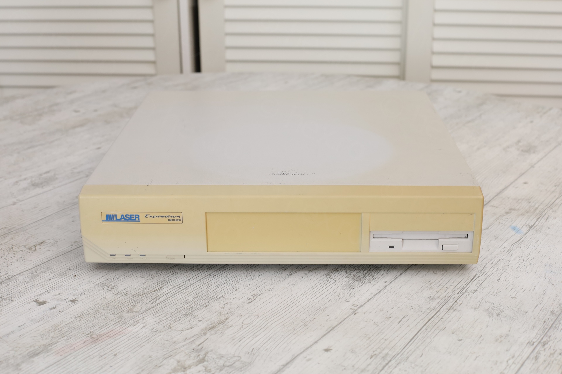
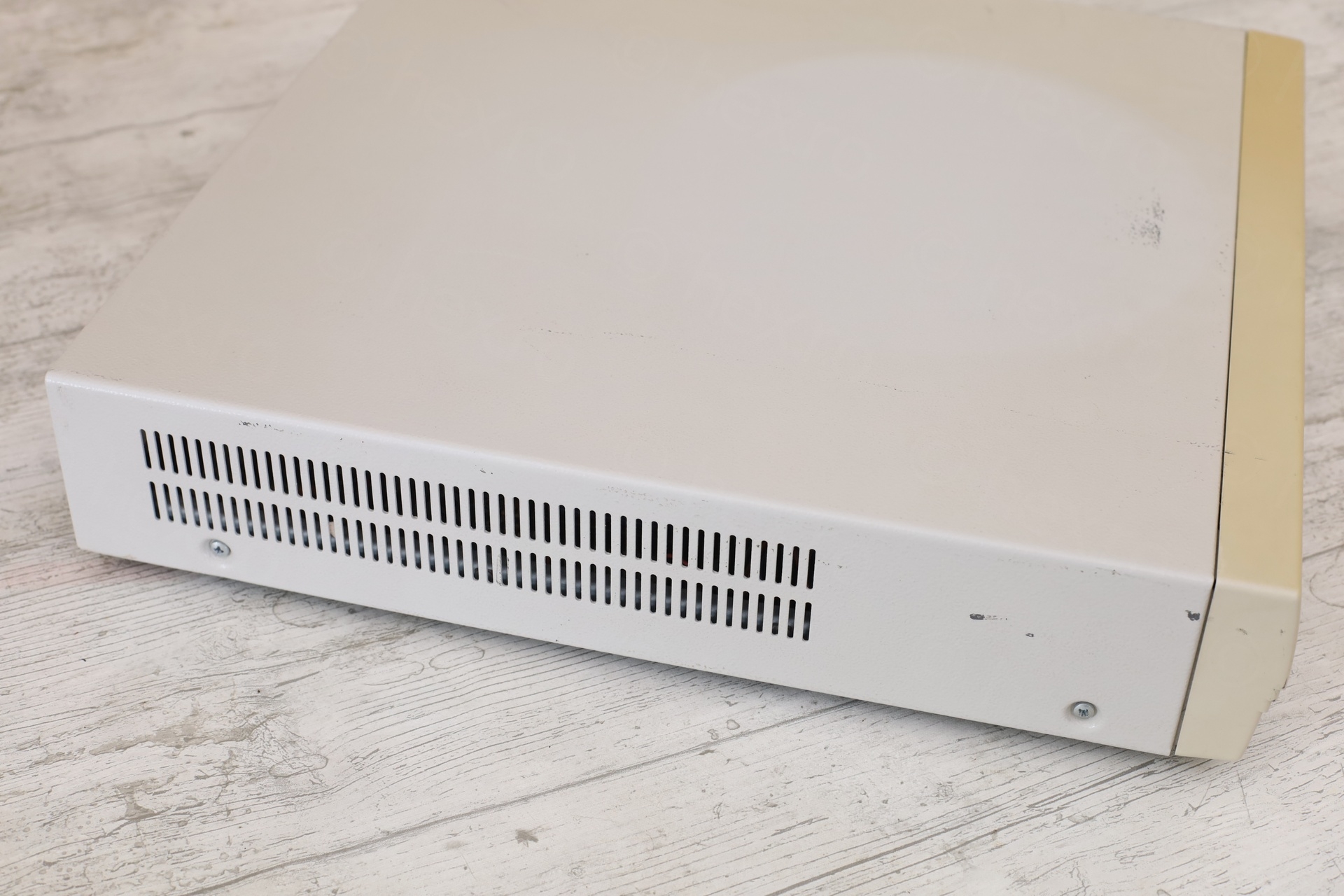
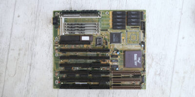
At home, I took it apart to have a look. Although the motherboard is a proprietary format (I am happy I got it with the matching case), it is nice that it already has a Video card built in. First thing I spotted was that there was a battery leak.
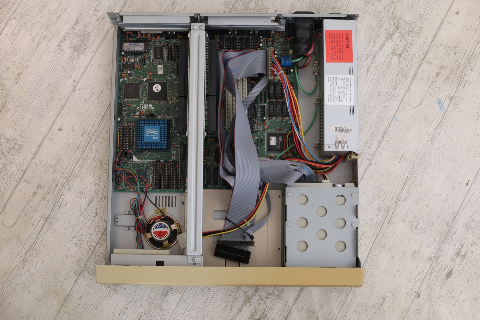
To take the motherboard out, the front panel of the case has to come out. Because there is a large piece of plastic, flat, that sits above the side of the motherboard, and you can’t lift it. Once the front panel comes out, this large plastic “retainer” can be slid out, releasing the motherboard:
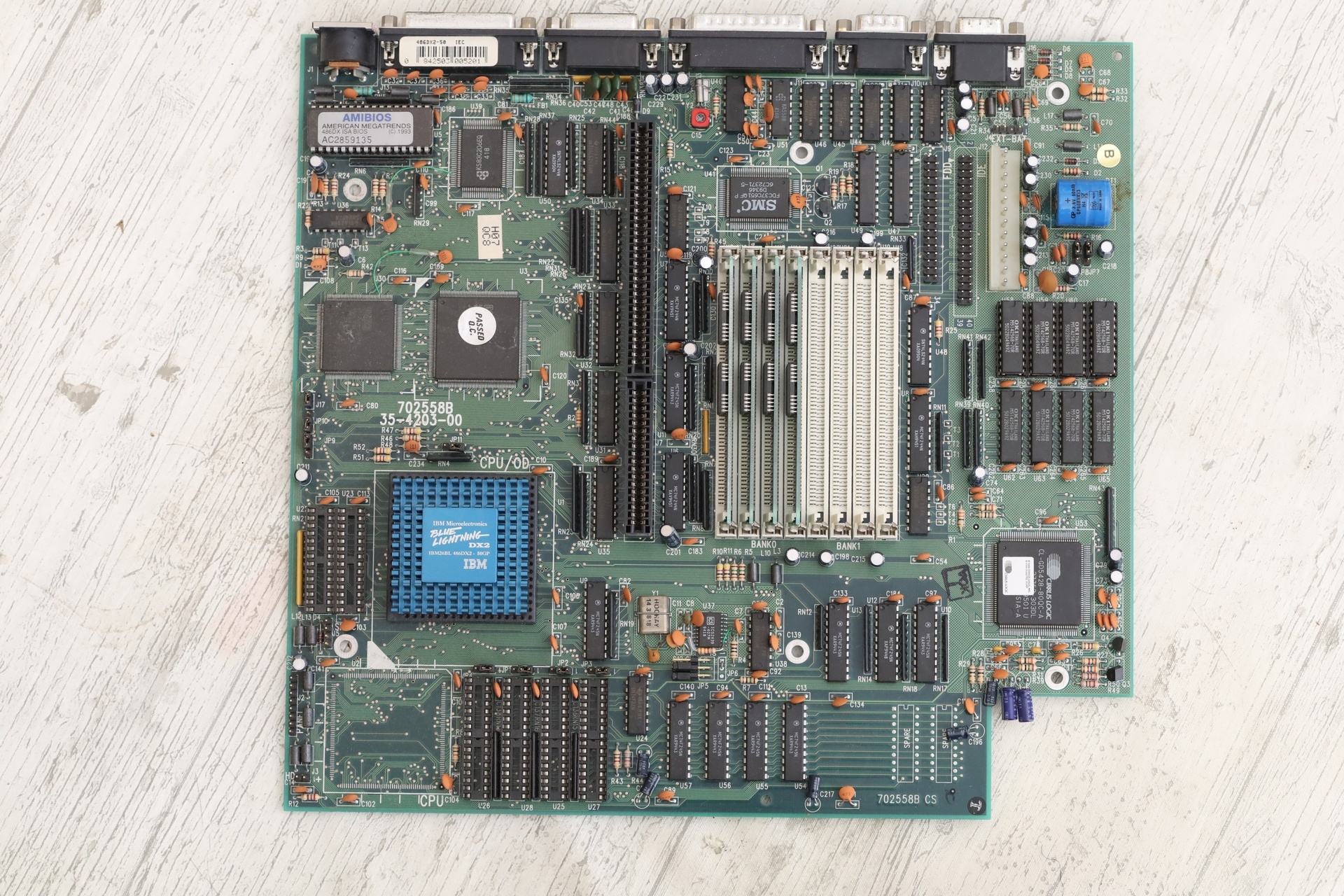
The specs are:
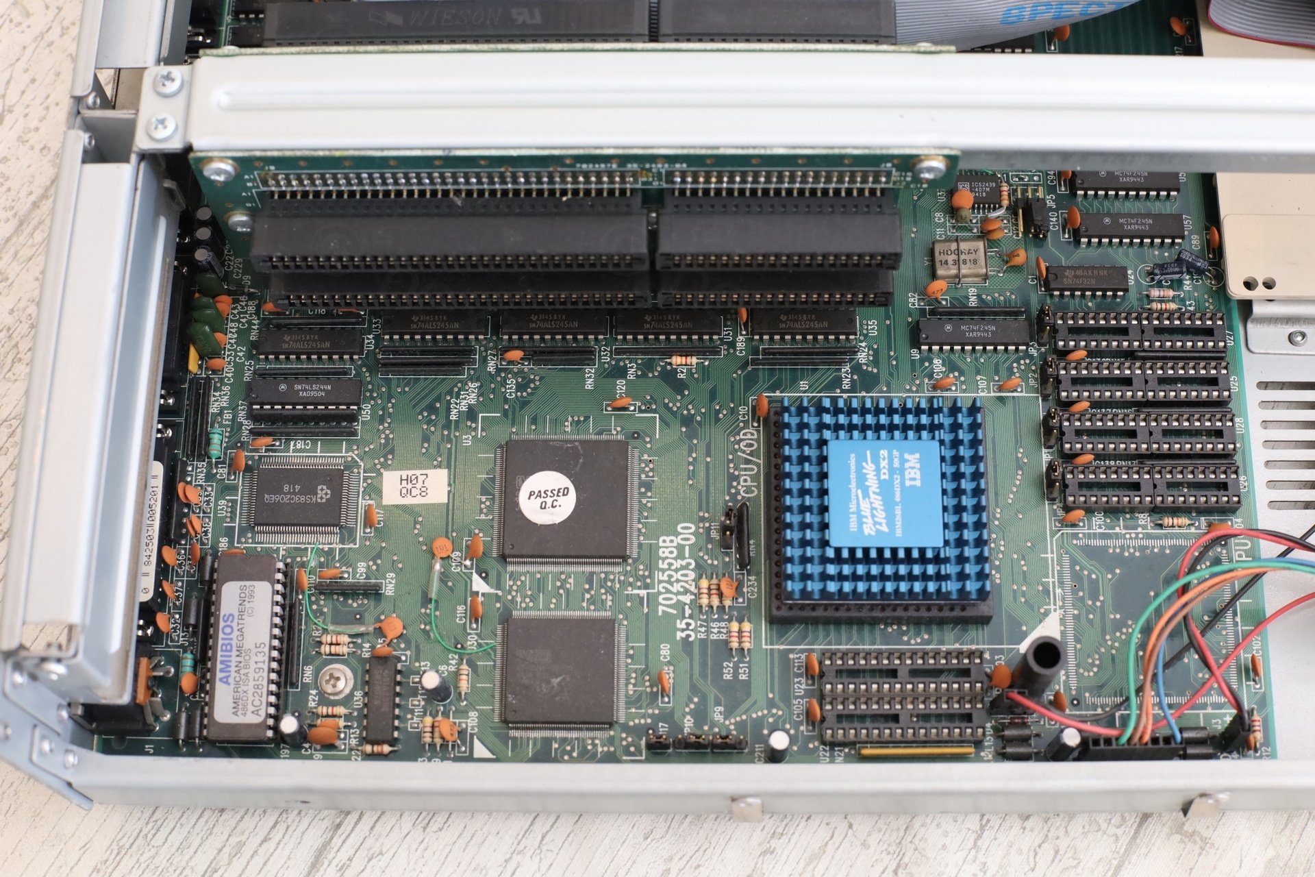
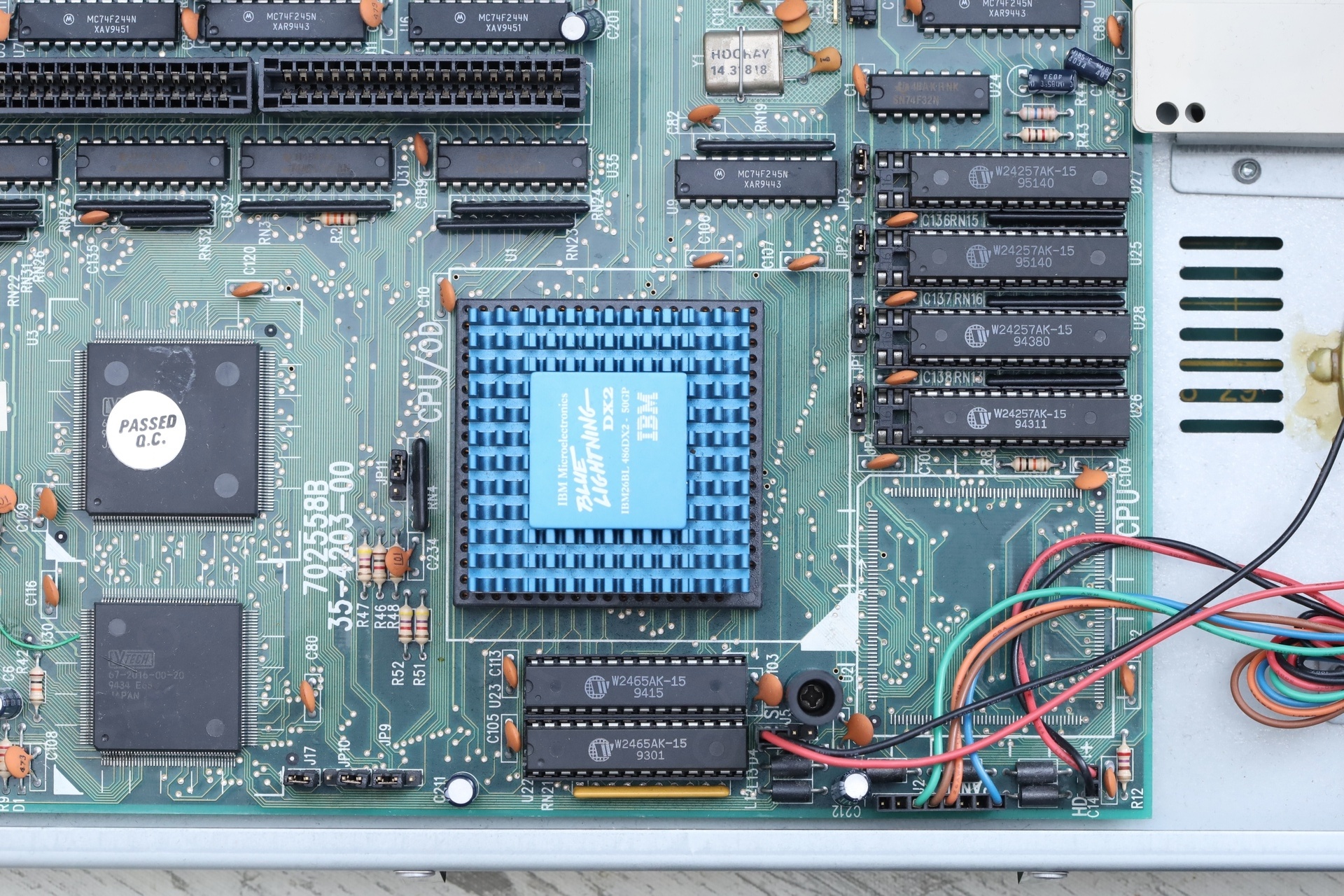
- Cyrix Cx486DX2-50 CPU (IBM Blue Lightning DX2)
- PCPartner 486 ASIC II Motherboard
- 4MB of RAM (4 x 1Mb SIMM 30 pin)
- Cirrus Logic GD5428 (1Mb of RAM)
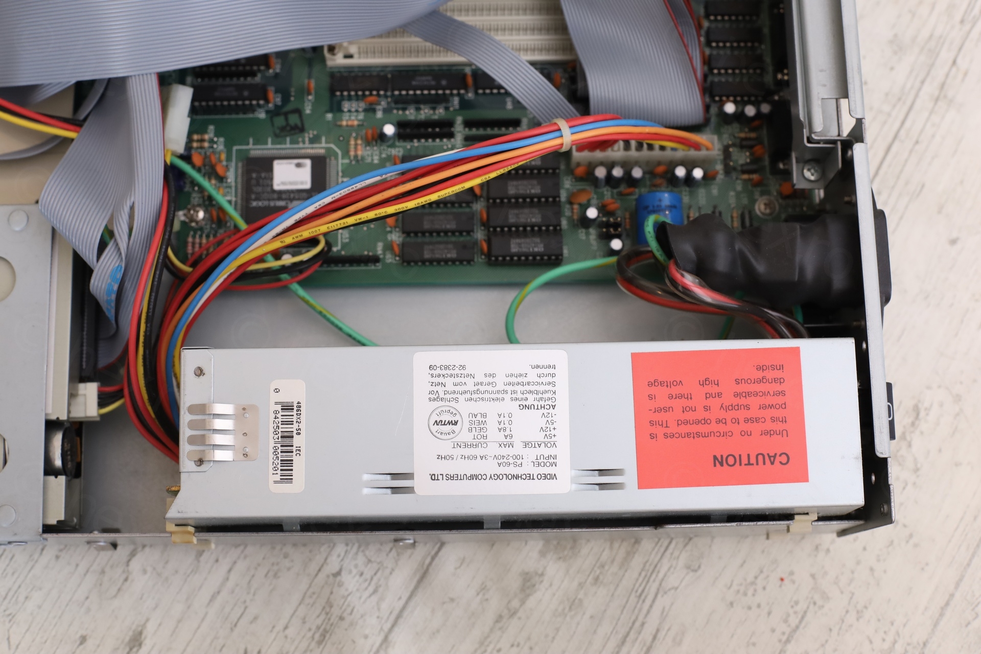
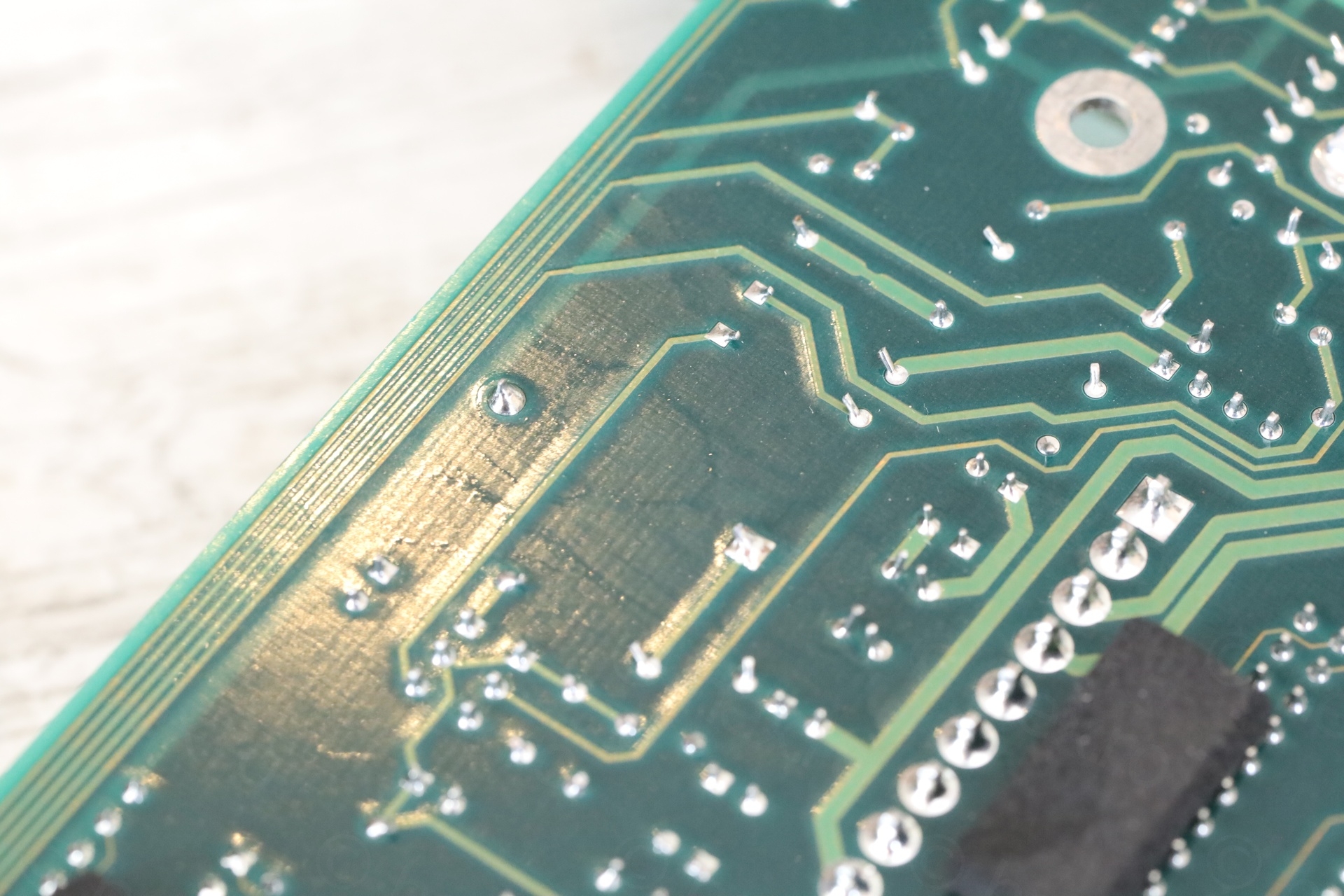
The motherboard looked a little dusty. And surprisingly, had a bunch of wires (including a germanium diode ?! and resistors) soldered on the back:
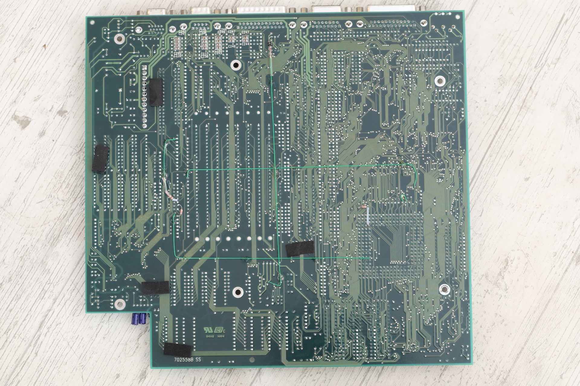
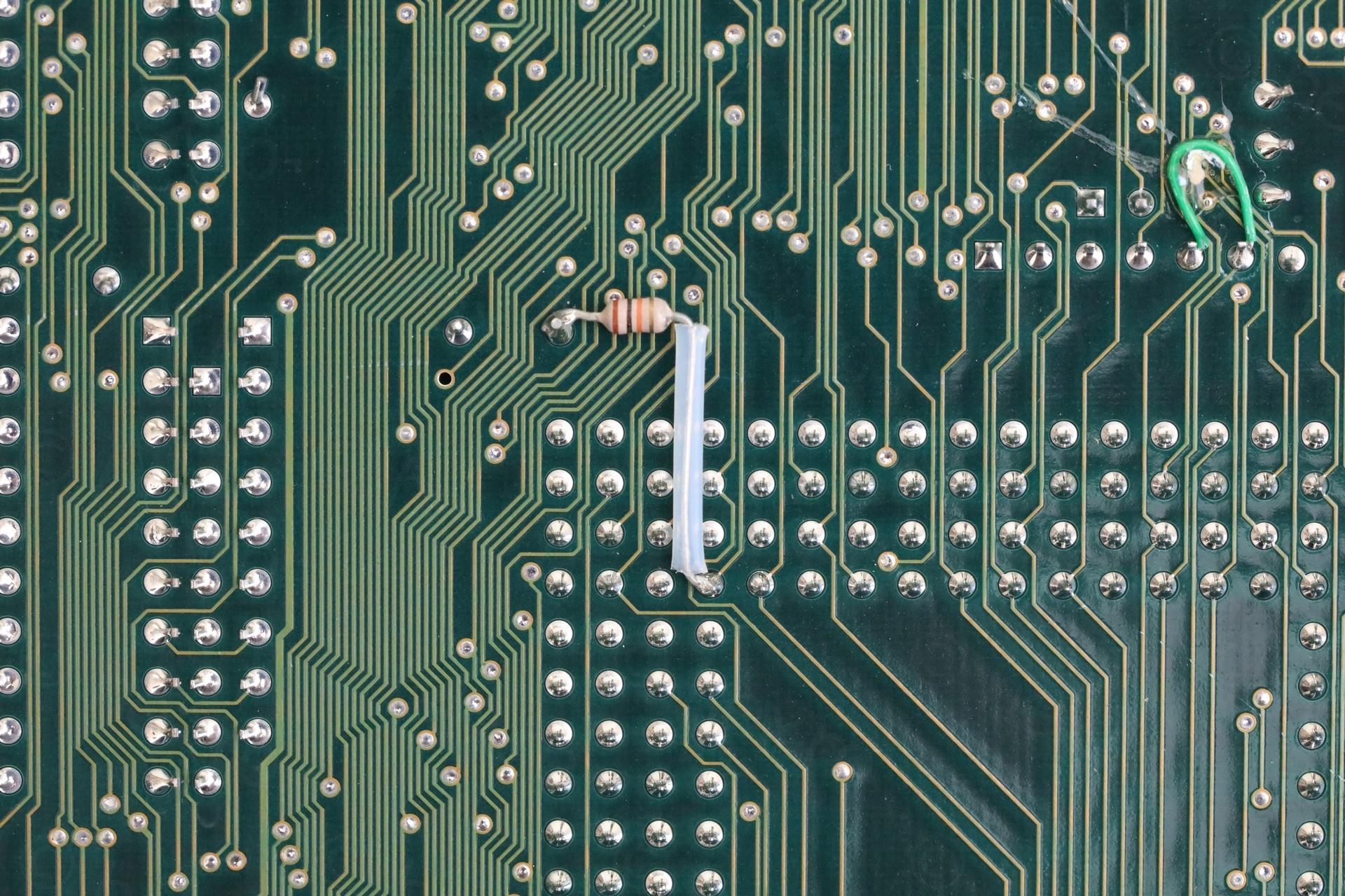
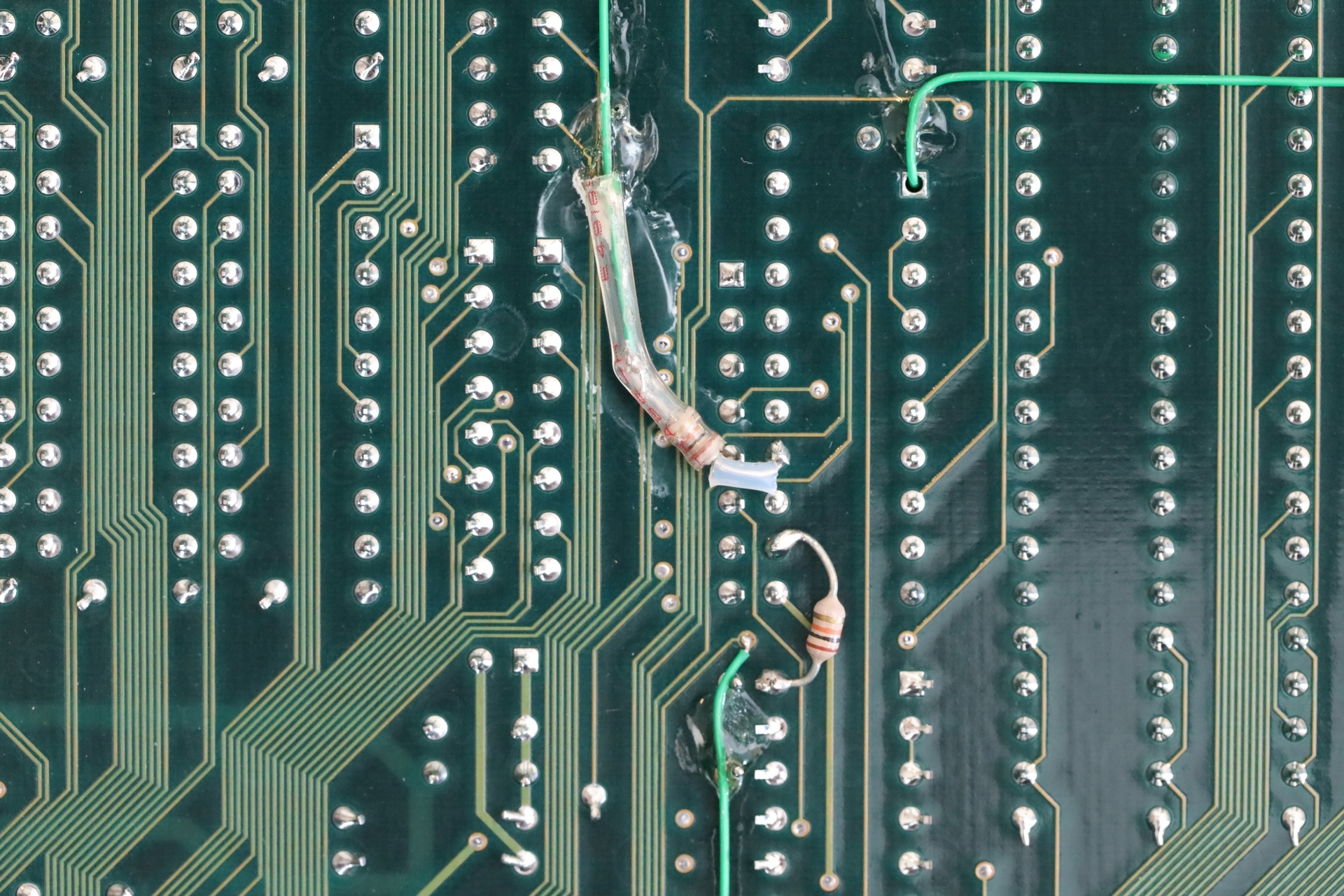
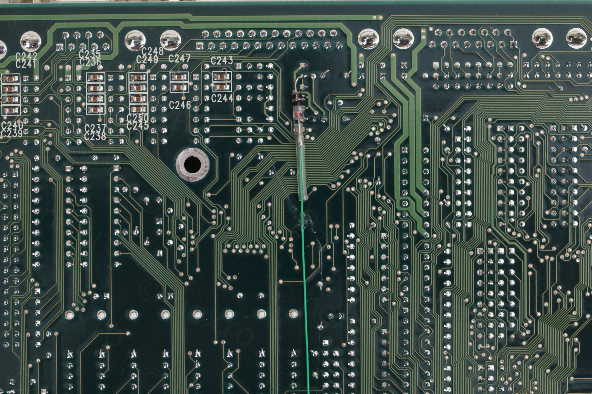
This was puzzling, but, looking around on the TheRetroWeb, I found a similar VTech chipset motherboard https://theretroweb.com/motherboards/s/pcpartner-35-2527-01-702496c-c0040-10-f (the image 2 of 7 from megatog615) also with green wires underneath. This was a relief. I was afraid the wires are some weird later mod, but they seem factory.
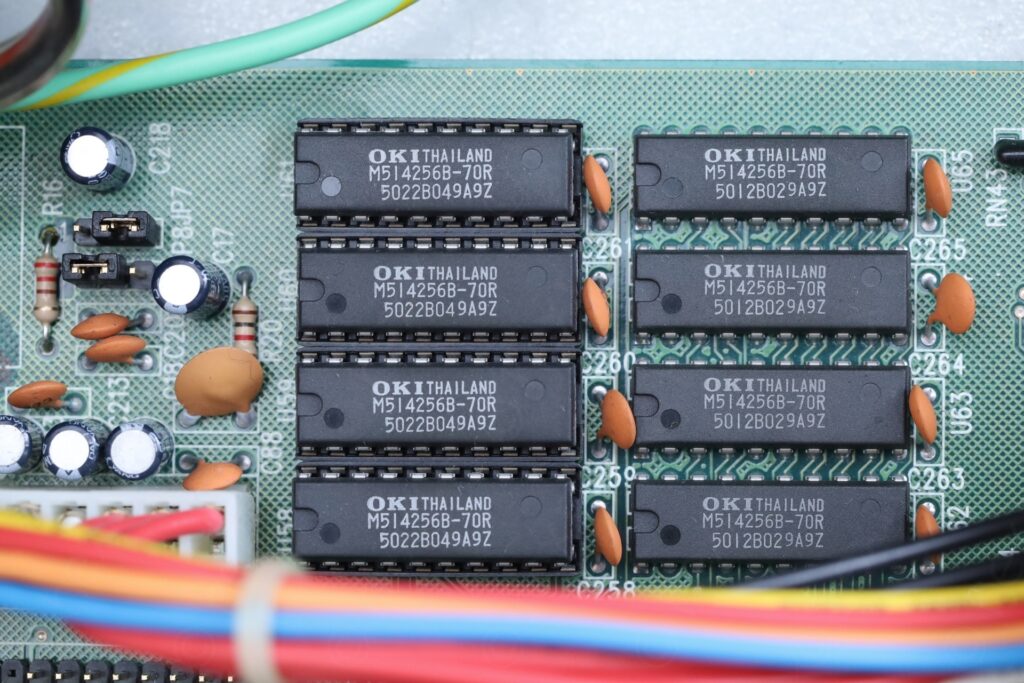
One nice surprise though was that while 512Kb of video memory is soldered, the expansion sockets (for an additional 512Kb) were already populated. All video memory ICs are OKI M514256B-70R.
External cache memory sockets were empty. While the manual states that motherboard supports 128Kb of Write-back secondary cache, I found no references on what chips to use. I managed to get it going, details will be below.
Battery leakage / cleanup
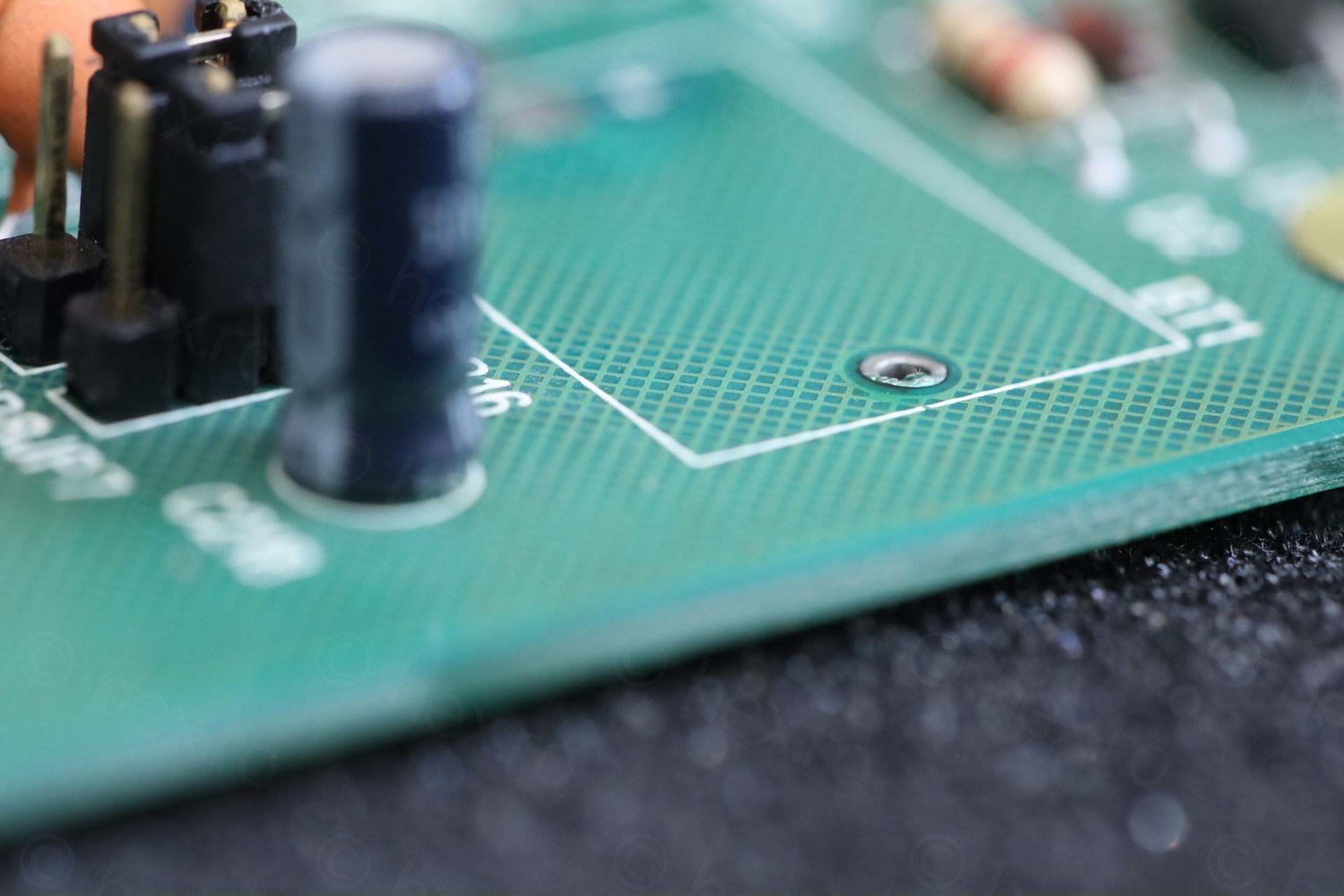
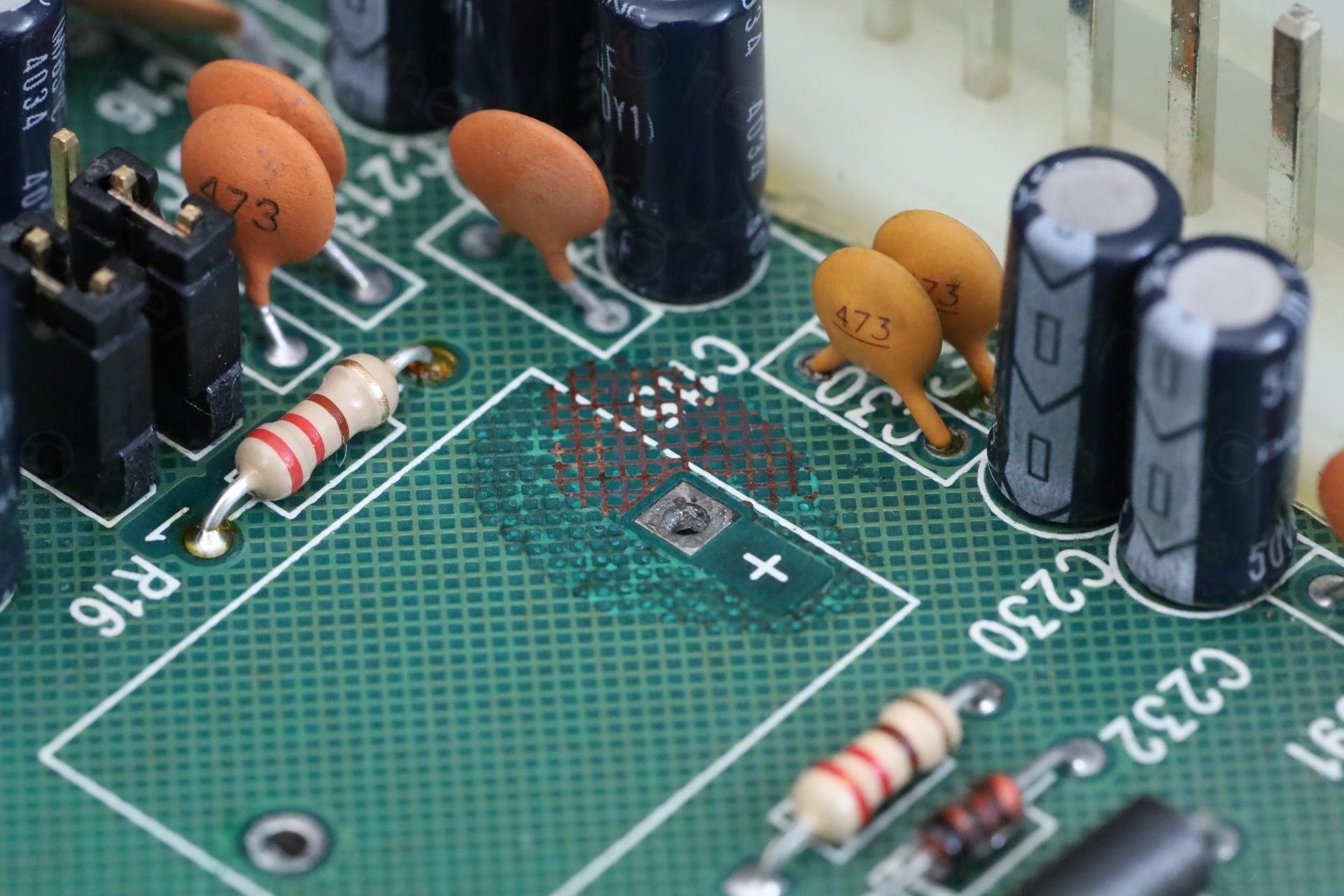
Only after reviewing the shots, I spotted a cracked ceramic capacitor nearby, as well as few more passive components with corroded leads. Looking carefully, the findings looked puzzling to me. There was some rosin / flux on the battery negative terminal and the pad was lifted already. Some smudges on the back of the board as if somebody tried to clean flux:
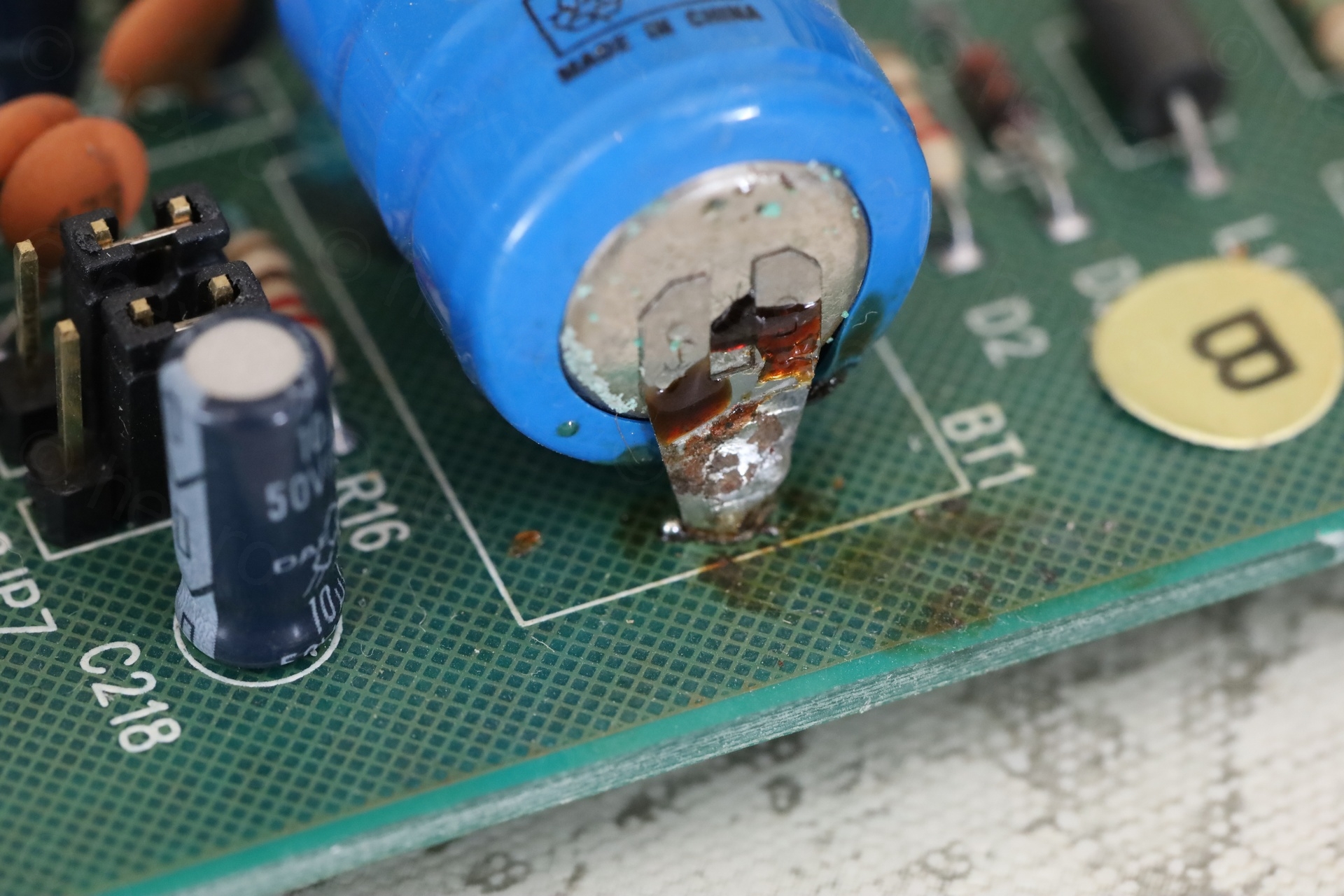
I suspect somebody replaced the battery a while back. As the replacement battery also corroded (you can corrosion oozing out from under the blue plastic film).
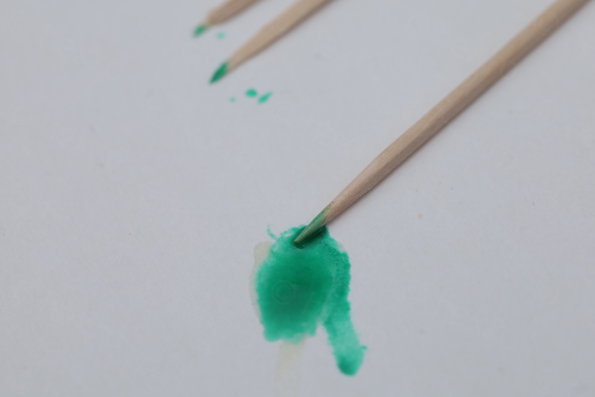
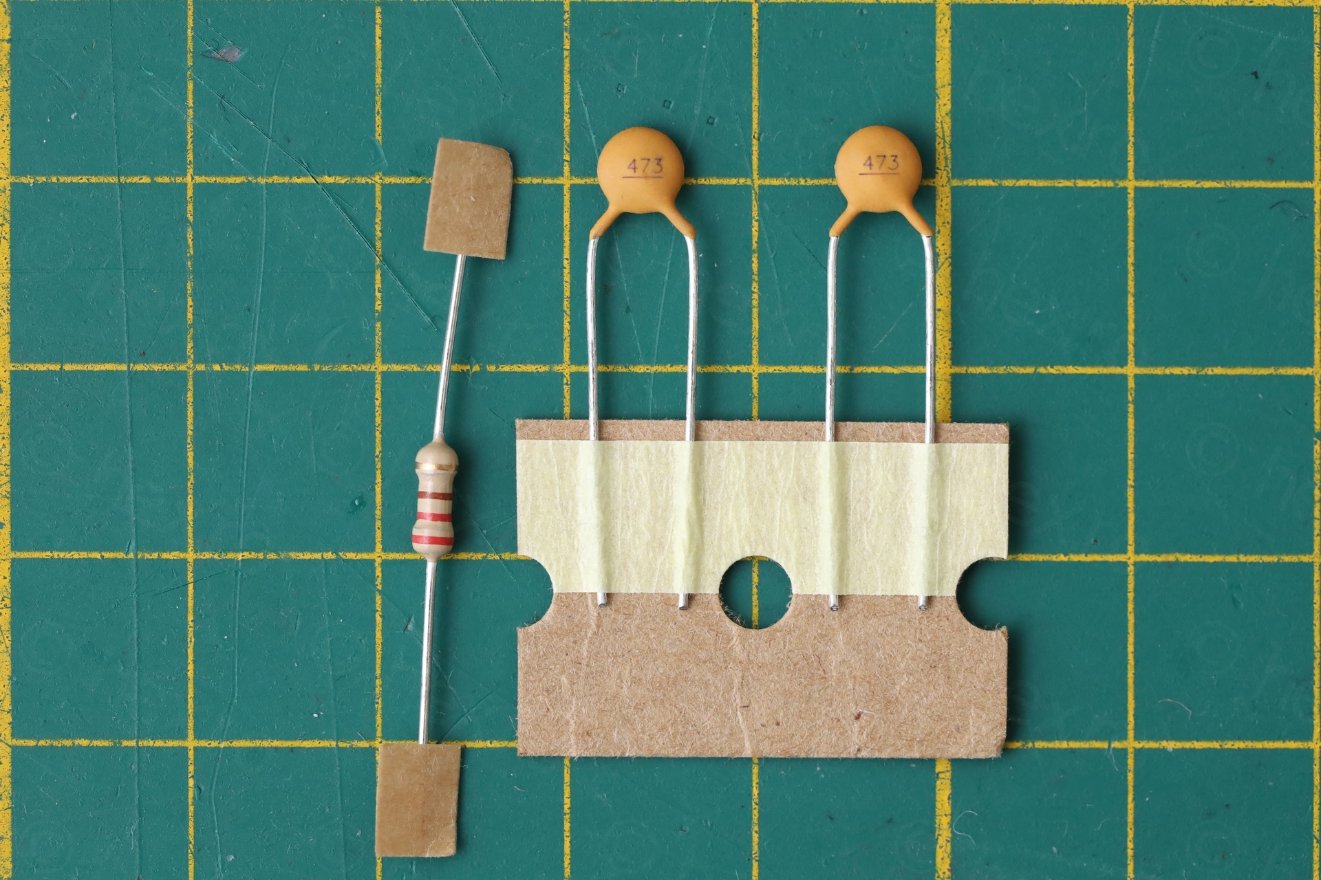
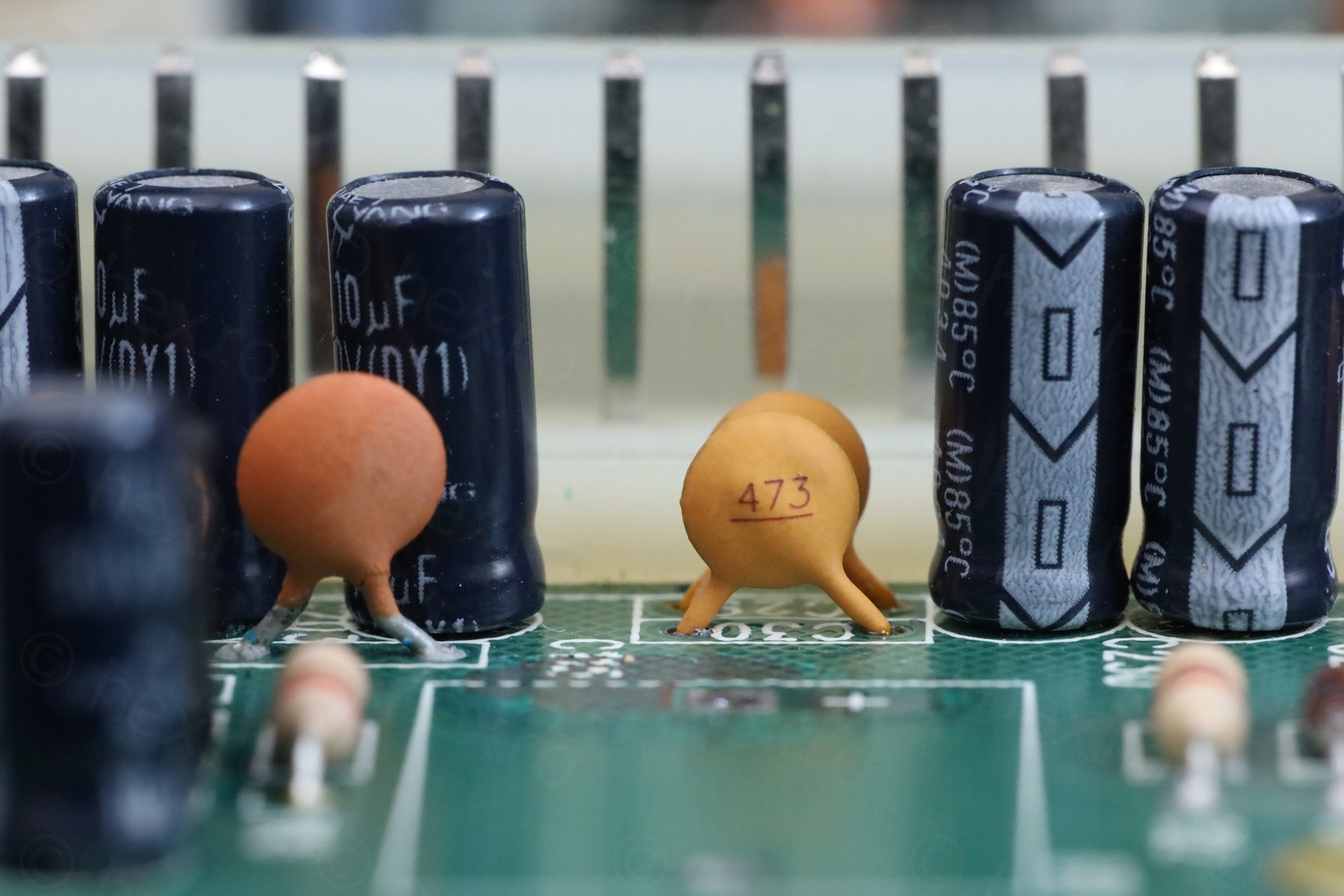
Thankfully, the markings on the passive components were visible: 473 for the affected ceramic capacitors and 220Ω for the nearby resistor. Cleanup was using vinegar to remove existing oxidation, wash everything out with Isopropylic alcohol and replace the affected components:
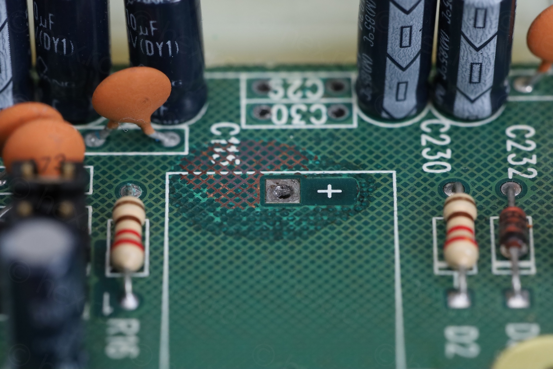
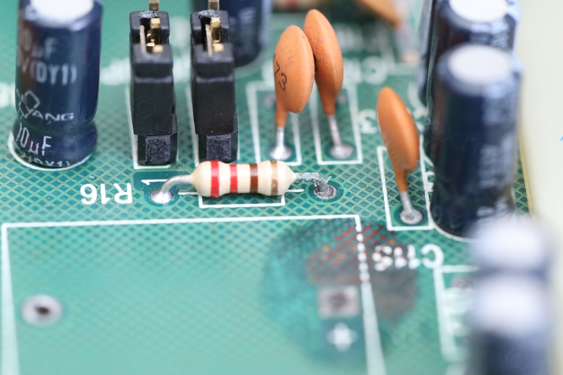
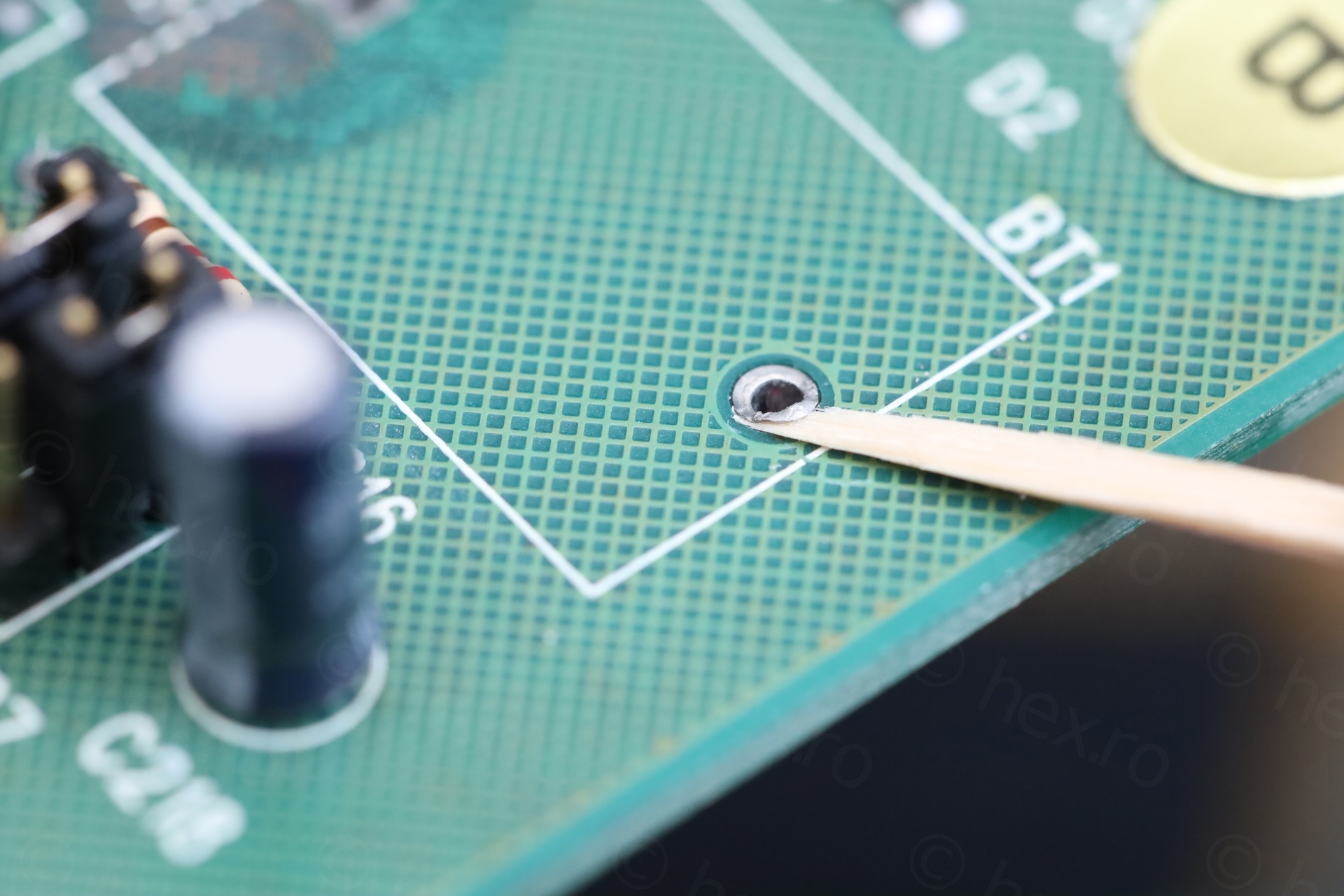
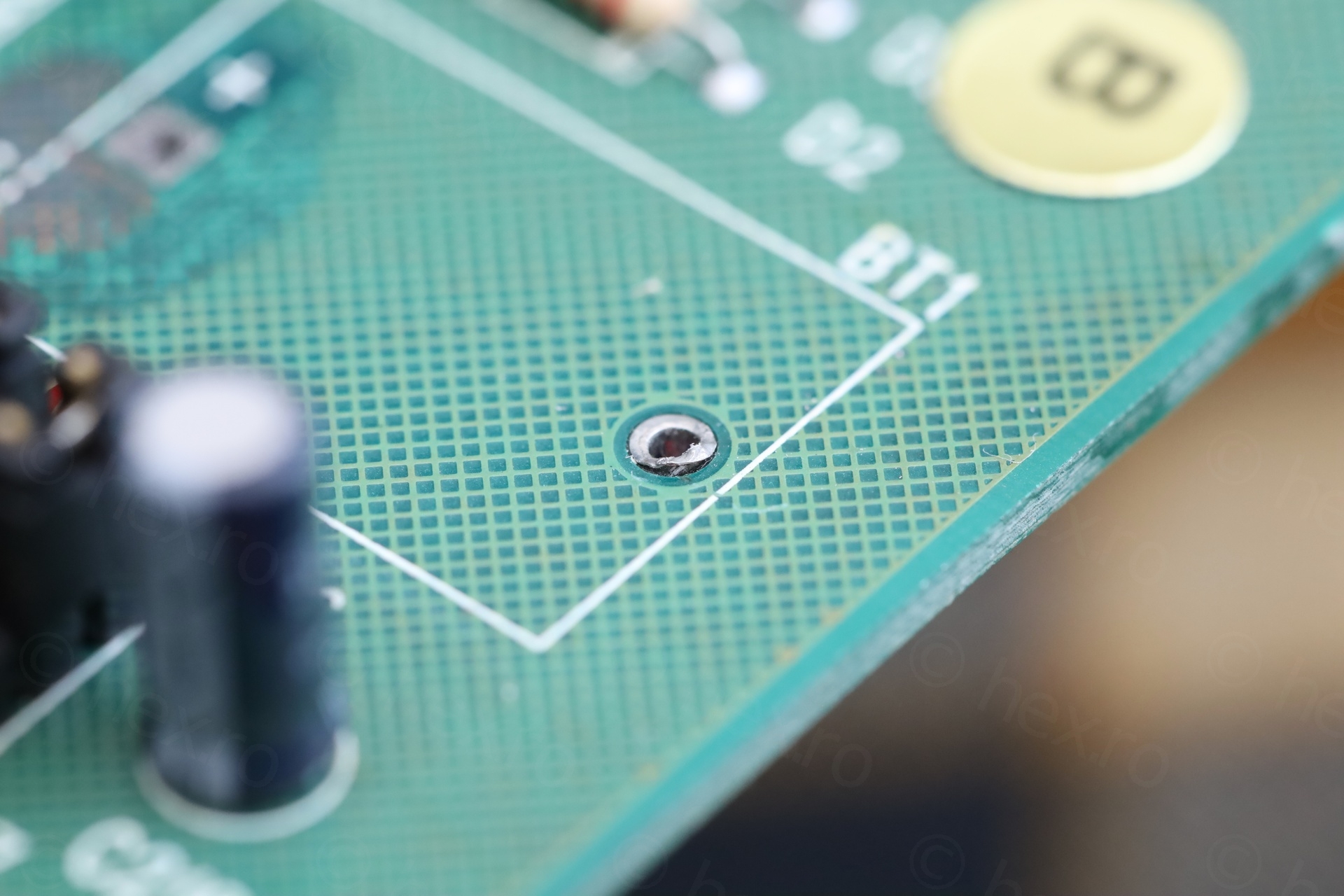

I repaired the lifted pad (just to make sure, using epoxy), and replaced the three corroded components:
DIY External Battery Pack
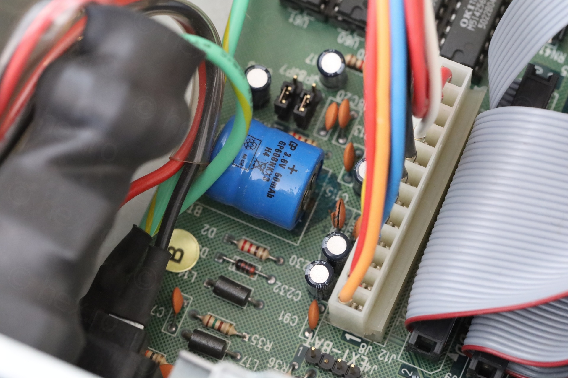
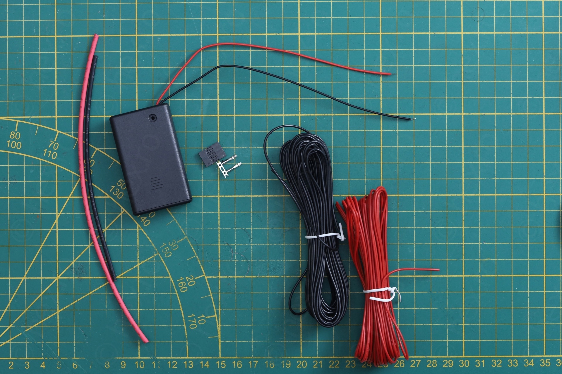
Although similar batteries are still available to buy, I didn’t – computer will stay more in storage than on my desk. Since this 486 board allows an external battery pack – why not building an external battery pack ?
I had no clue what voltage is needed. There is a diode in series with the positive pin of the 4 pin external battery pack. I did some tests with 3 x AAA batteries and seemed to run fine, so I ordered some holders and Dupont connectors and made 3 of them in total:
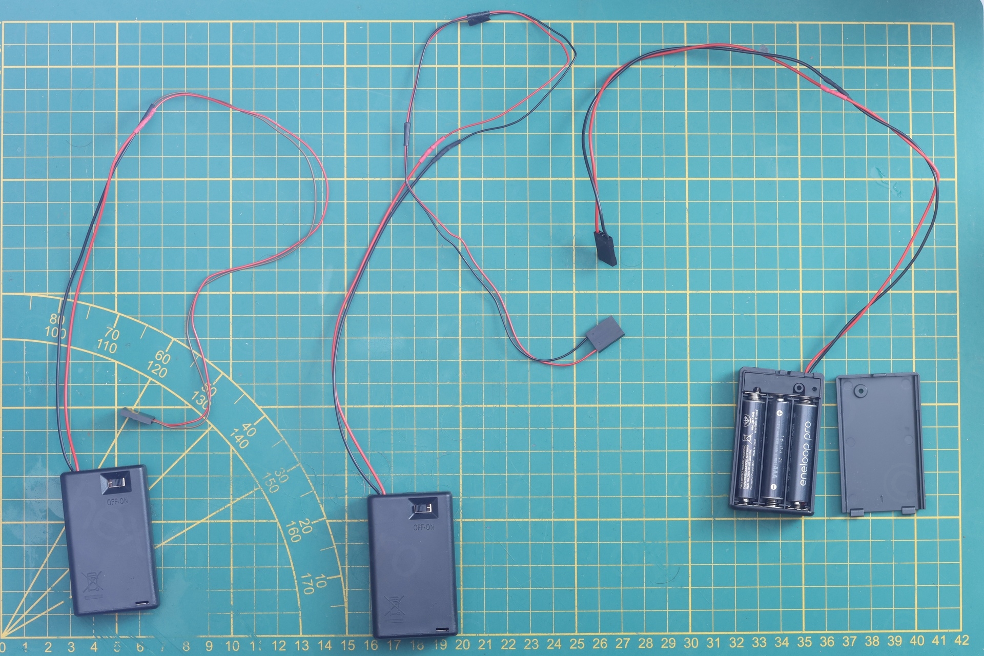
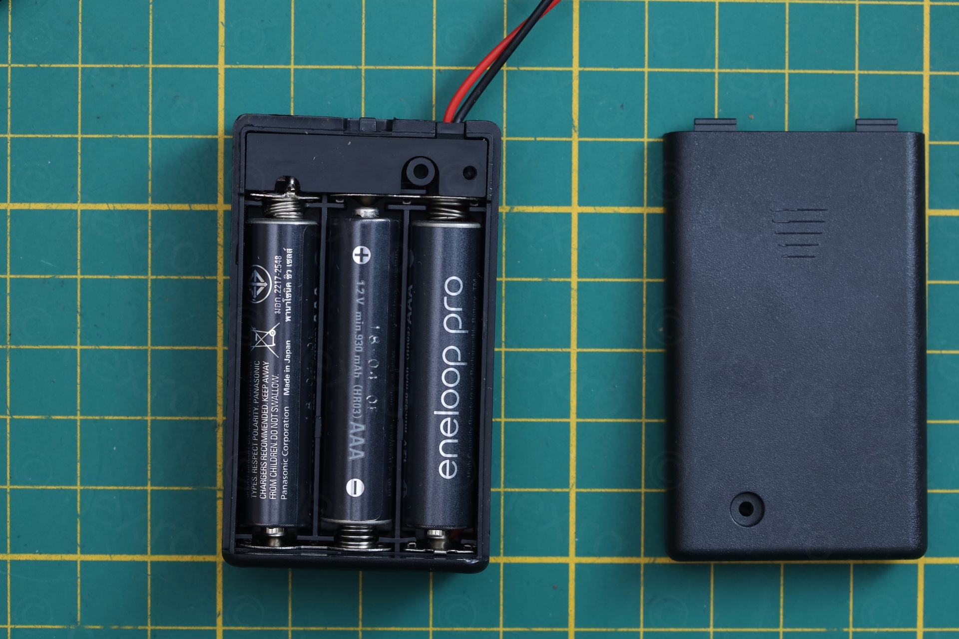
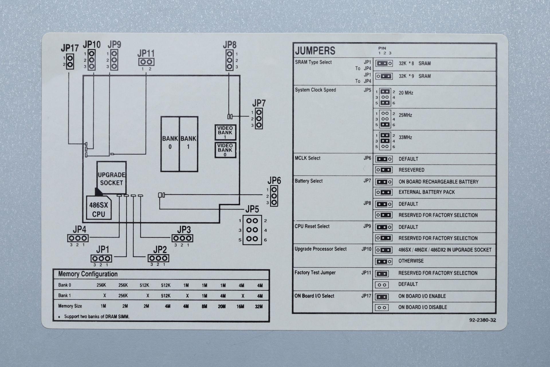
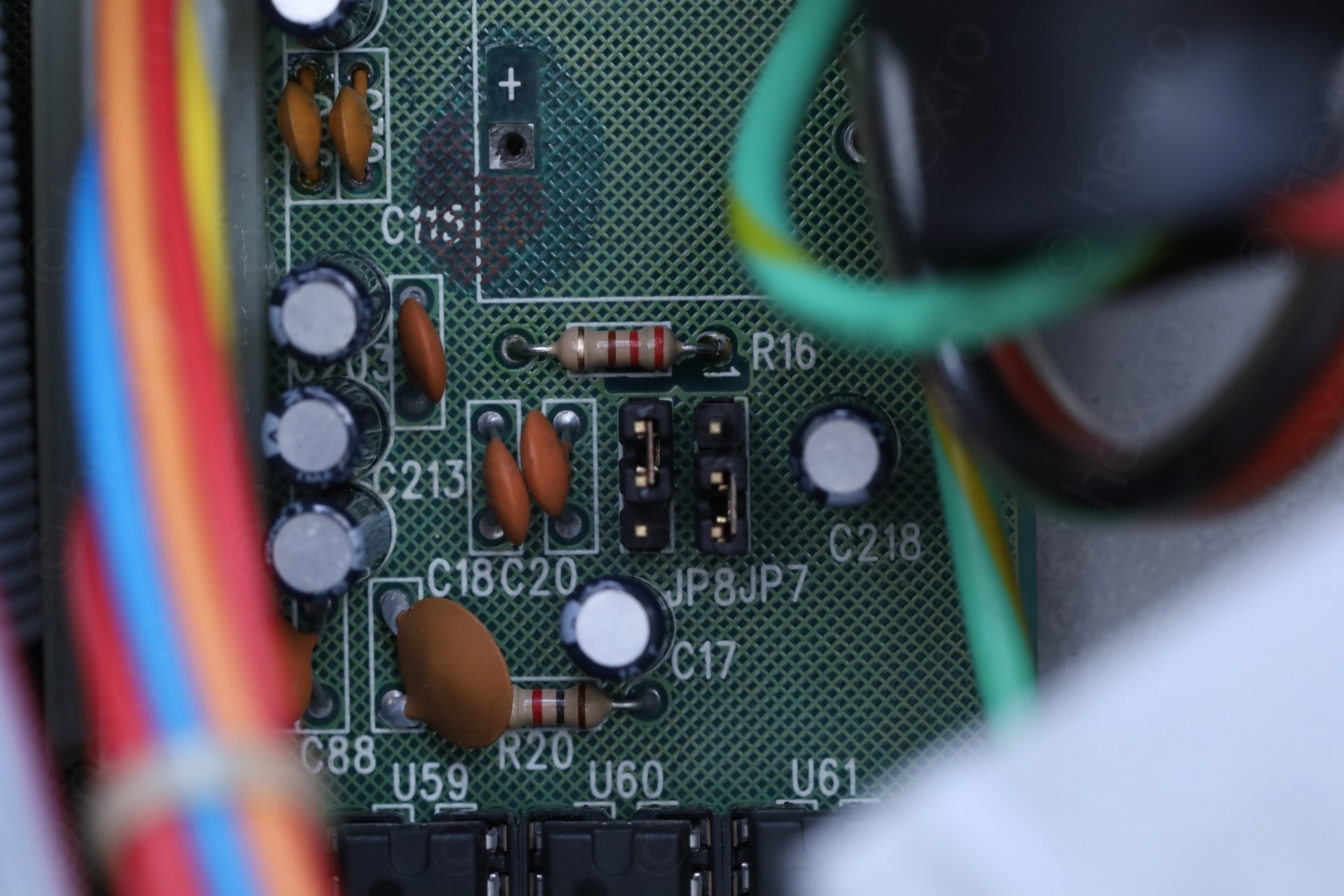
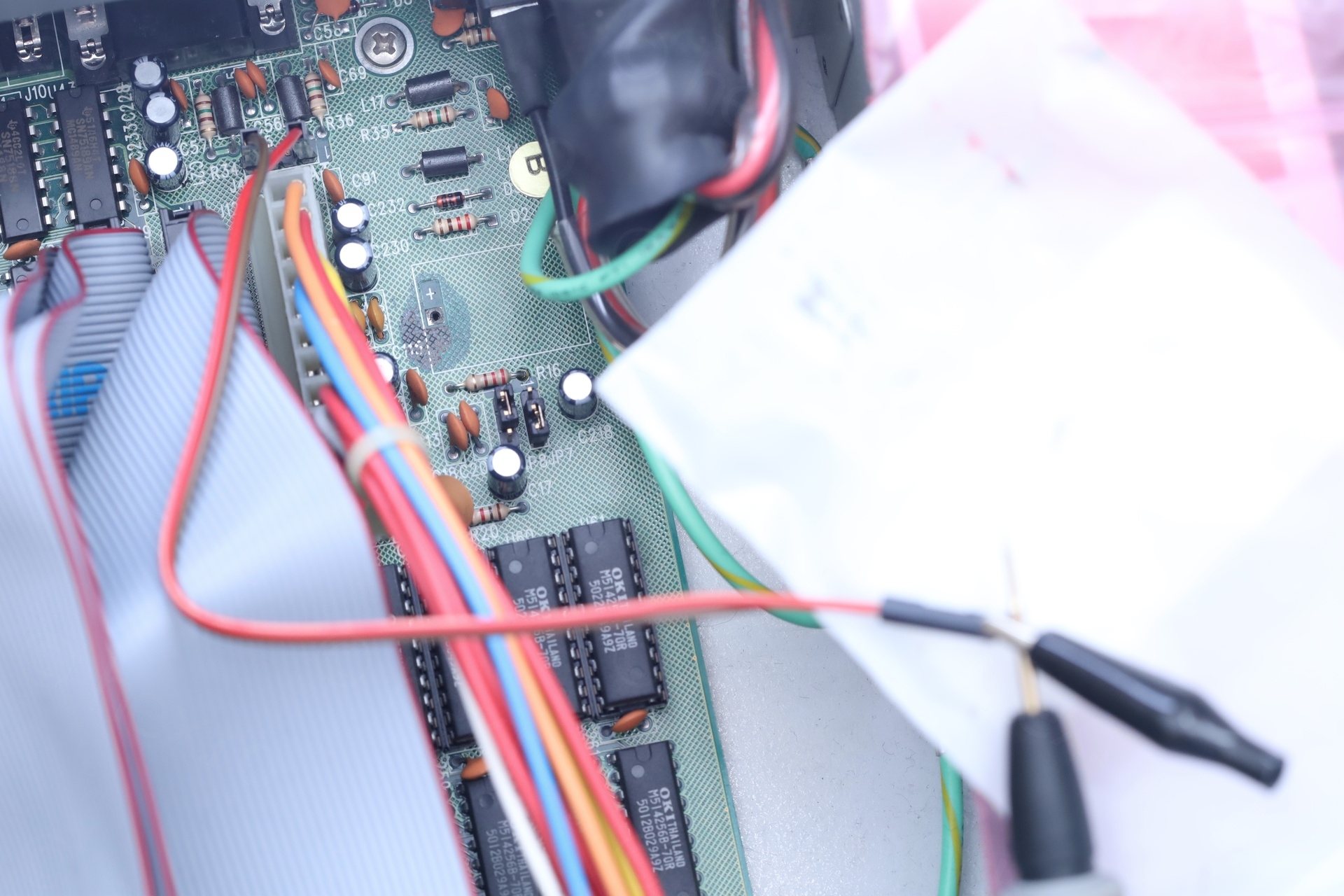
I will leave one in the computer thus, when I need it, I will just put some batteries and use it. JP7 has to be set so that the board uses the external battery pack:
With 3 x AAA rechargeable batteries, the pack shows 3.892V – and the current draw is 33.9µA. In fact, just after computer shutdown, the current draw is 33.8µA, but seems to slowly drop, saw also 33.4µA:
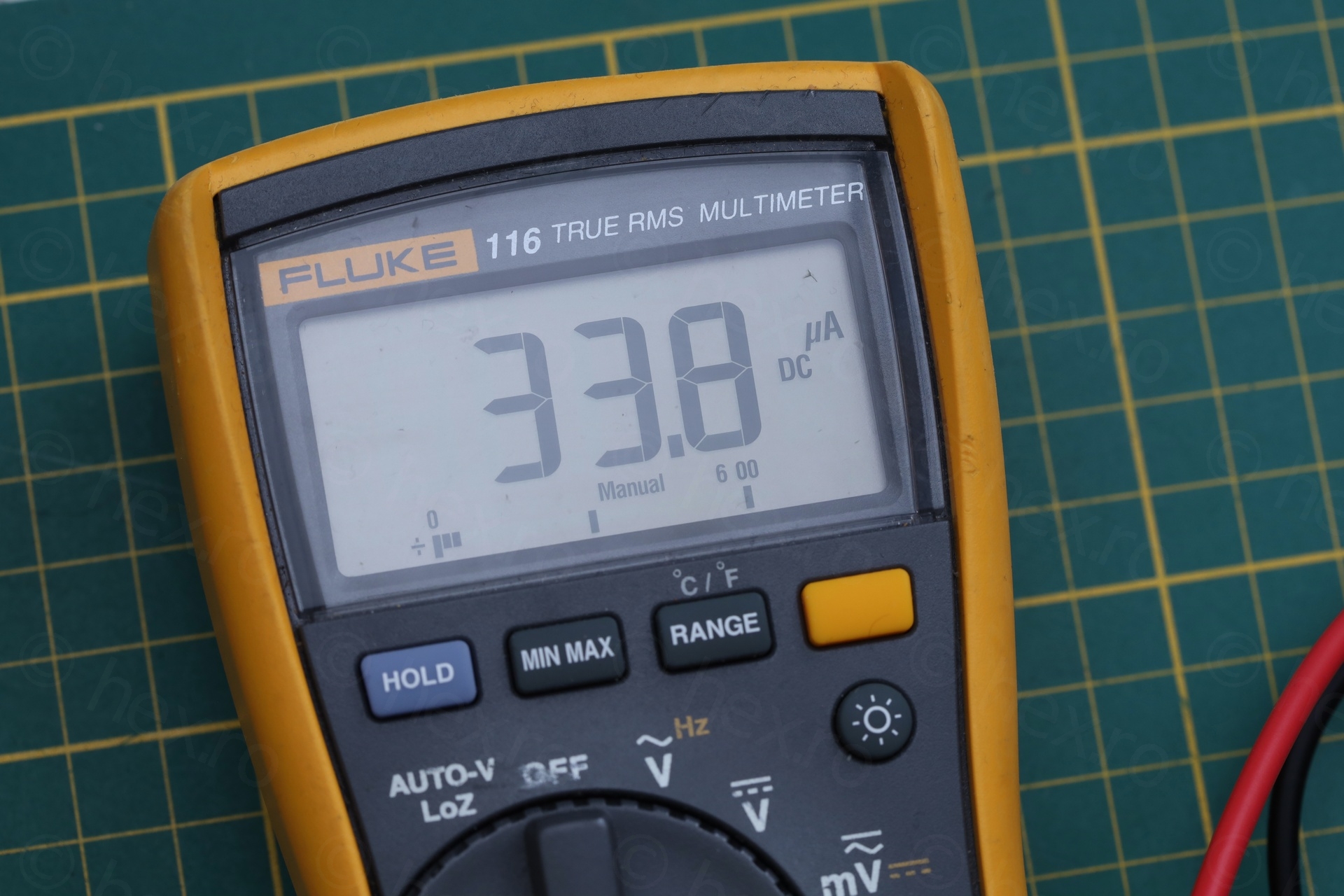
If a ideal battery has 900mAh capacity, it will last about 3 years at a 34µA current draw, assuming no other losses inside the battery, etc. Thus, this is good enough – especially with the zero risk of batteries leaking in the future (since I’m not going to leave them in 🙂 ).
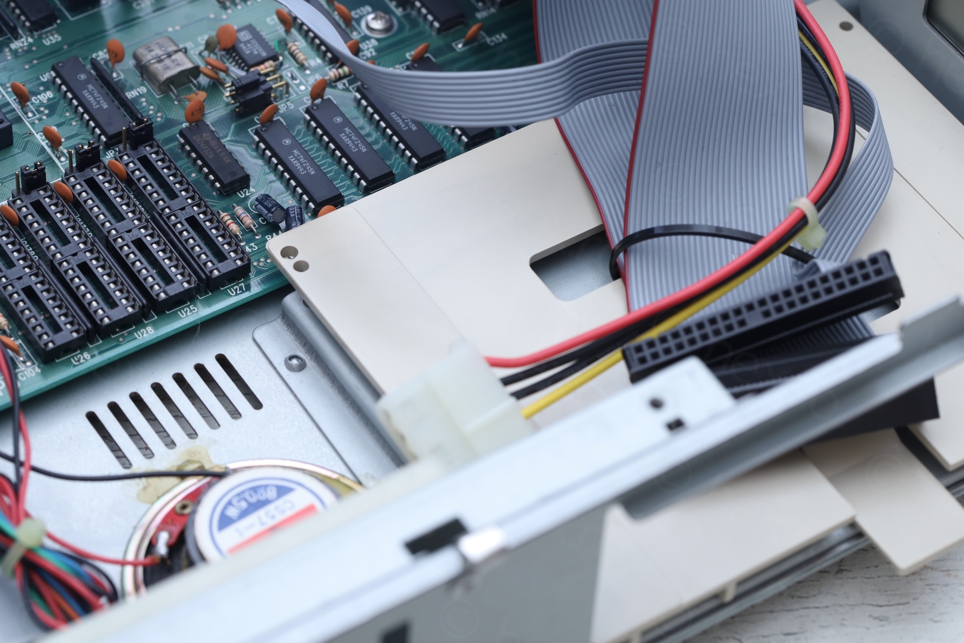
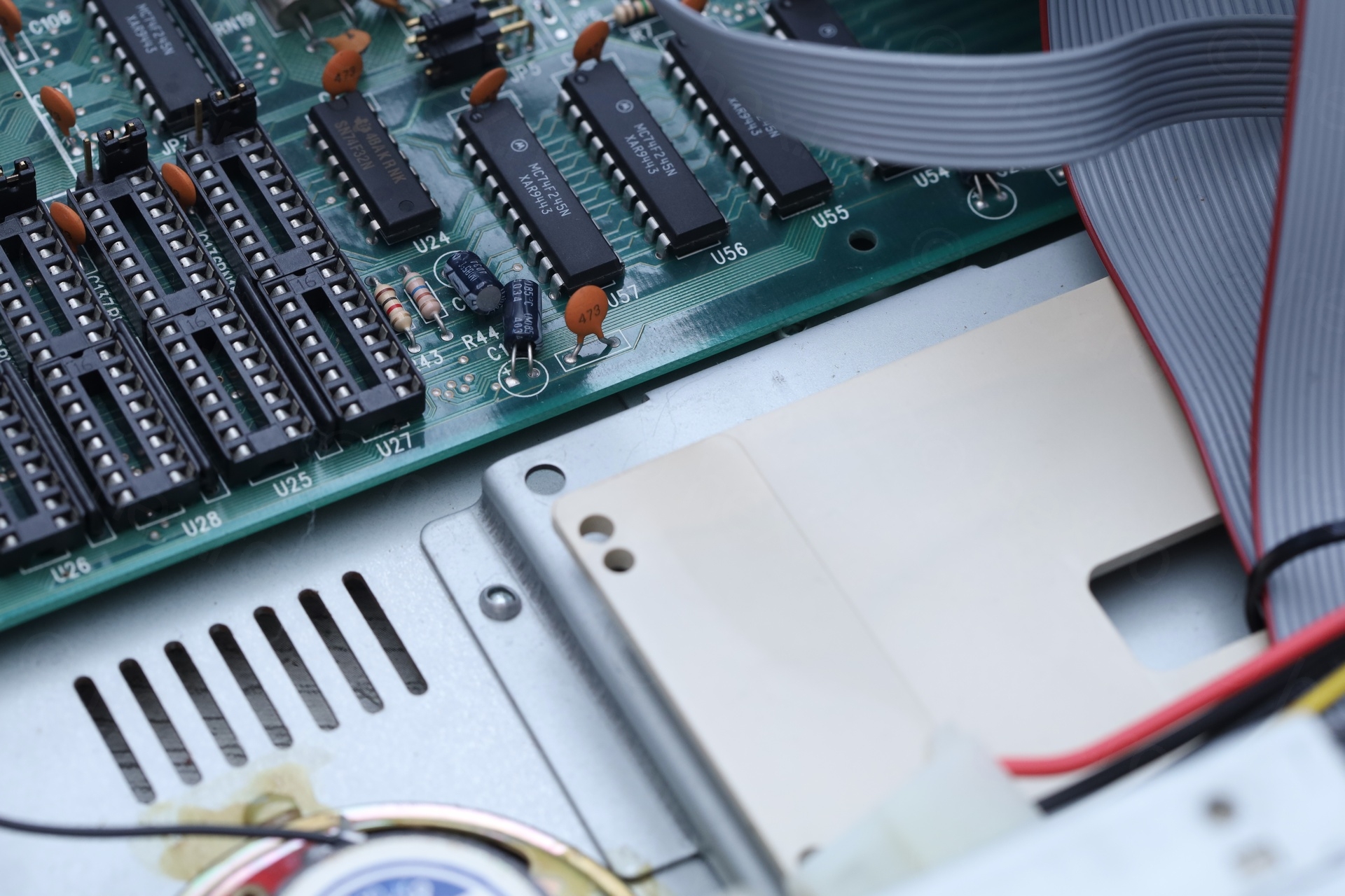
Populating the External Cache memory sockets
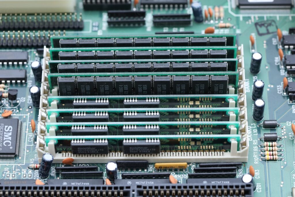
I was able to add 4 x 1Mb SIMM modules and fill out the memory sockets. And video memory sockets were already populated.
But what to do about the empty sockets for the cache memory ? It felt imperative to fill them!
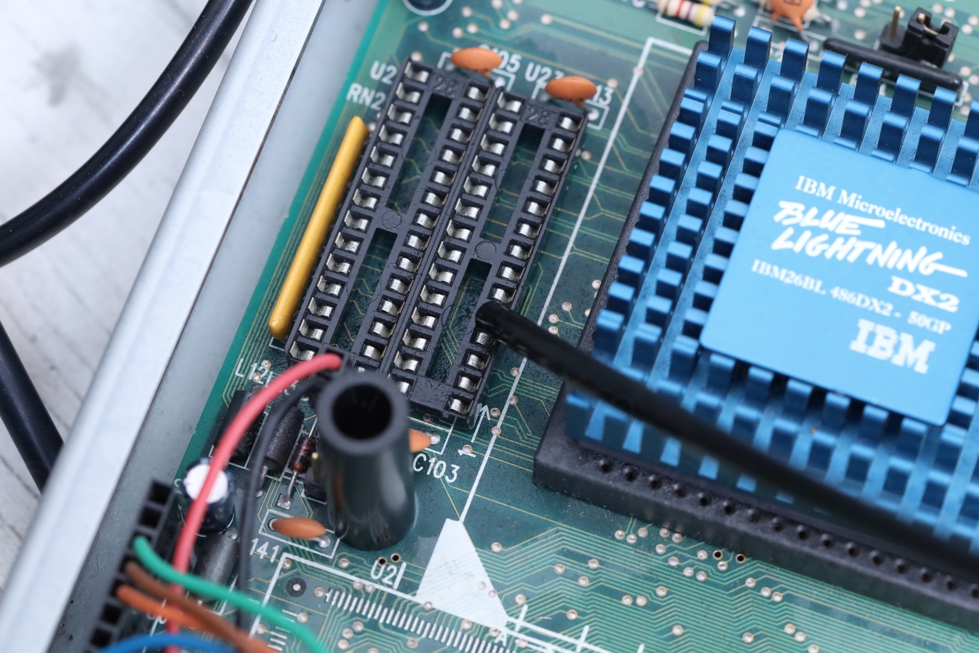
Where to start ? I assumed the empty sockets are for the external cache – but without markings on the board – it felt a bit risky. Also, there were 2 more empty sockets next to the CPU, what do they do, what are they for ?! Motherboard manual states that it supports 128Kb of external cache. Most online websites explain that a single TAG chip is needed to access this cache. Assuming one of the sockets next to the CPU is for the TAG chip, what is the purpose of the other socket ?

For the two sockets, I checked all the VTech motherboards on TheRetroWeb, and found a very interesting one: https://theretroweb.com/motherboards/s/pcpartner-35-8165-00-702585b-for-laser-2 with the same chips: VTech 67-2016-00-20 (ATU2) VTech 67-2017-00-20 (MC2)
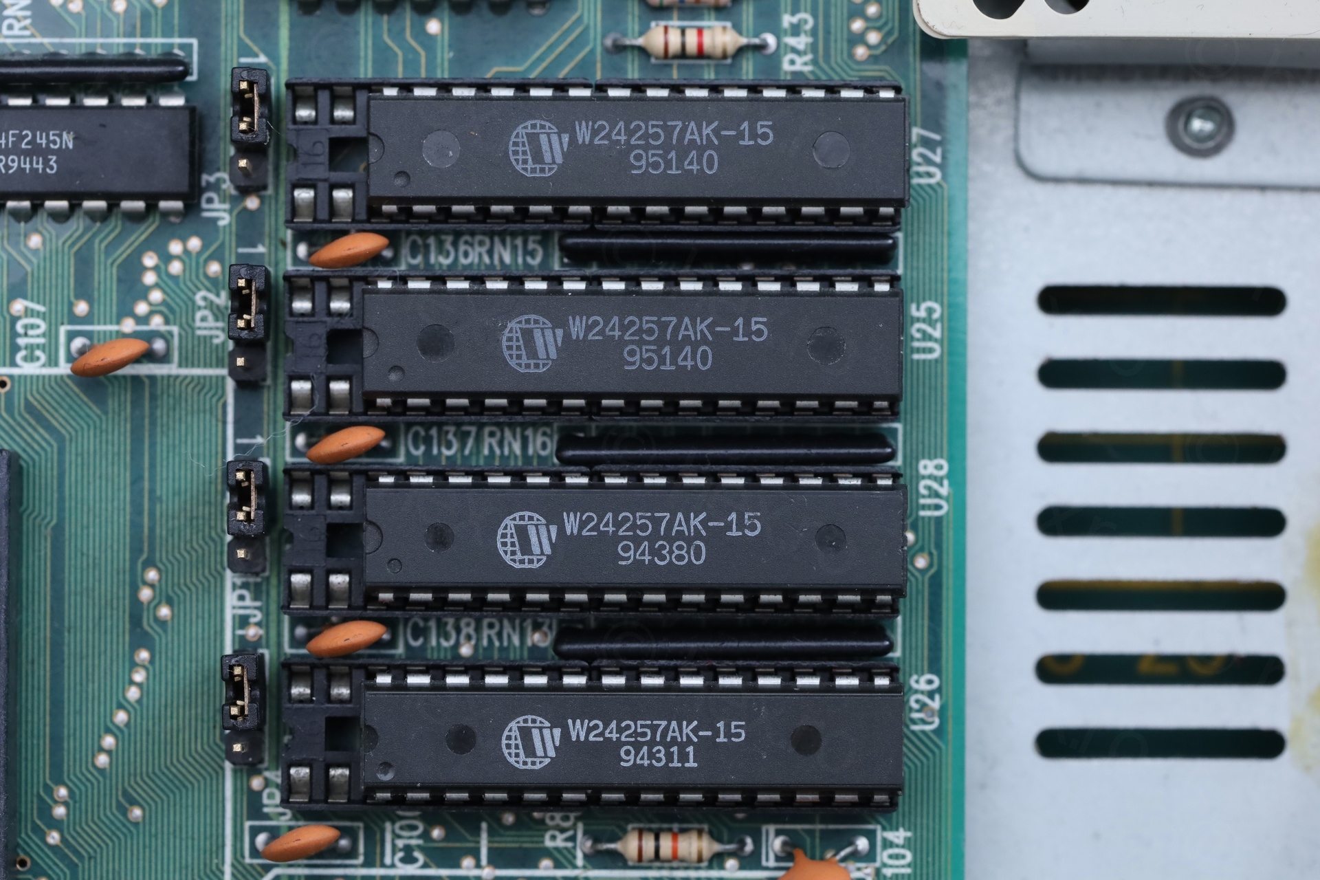
Interesting because it too had two additional sockets next to the CPU. Not only this, it also has label “TAG” label was next to them! The 4 sockets for the cache memory are have the label “DATA CACHE”. Okey!
As confirmation, I kept looking for boards with PGA168 CPU socket and with manuals. Many board were only having jumper settings, however, on page 2 of TheRetroWeb, I found this one: https://theretroweb.com/motherboards/s/ecs-um486-vio-d4m-rev-1-0#docs that has a manual in French.
Page 10 clarifies that for 128kb only 1 tag chip is needed.
How come my motherboard says it supports 128kb of L2 cache, but it provides TWO sockets for what I believe is for TAG chips ? It should only provide for one ? What is the use of the second one ? And what ICs to buy, in fact ? So many unknowns.
I then remembered a video from Bits und Bolts channel, where he shows several ICs that can be used for cache:
w24512AK-10
w24257AK-15
is61c1024-10
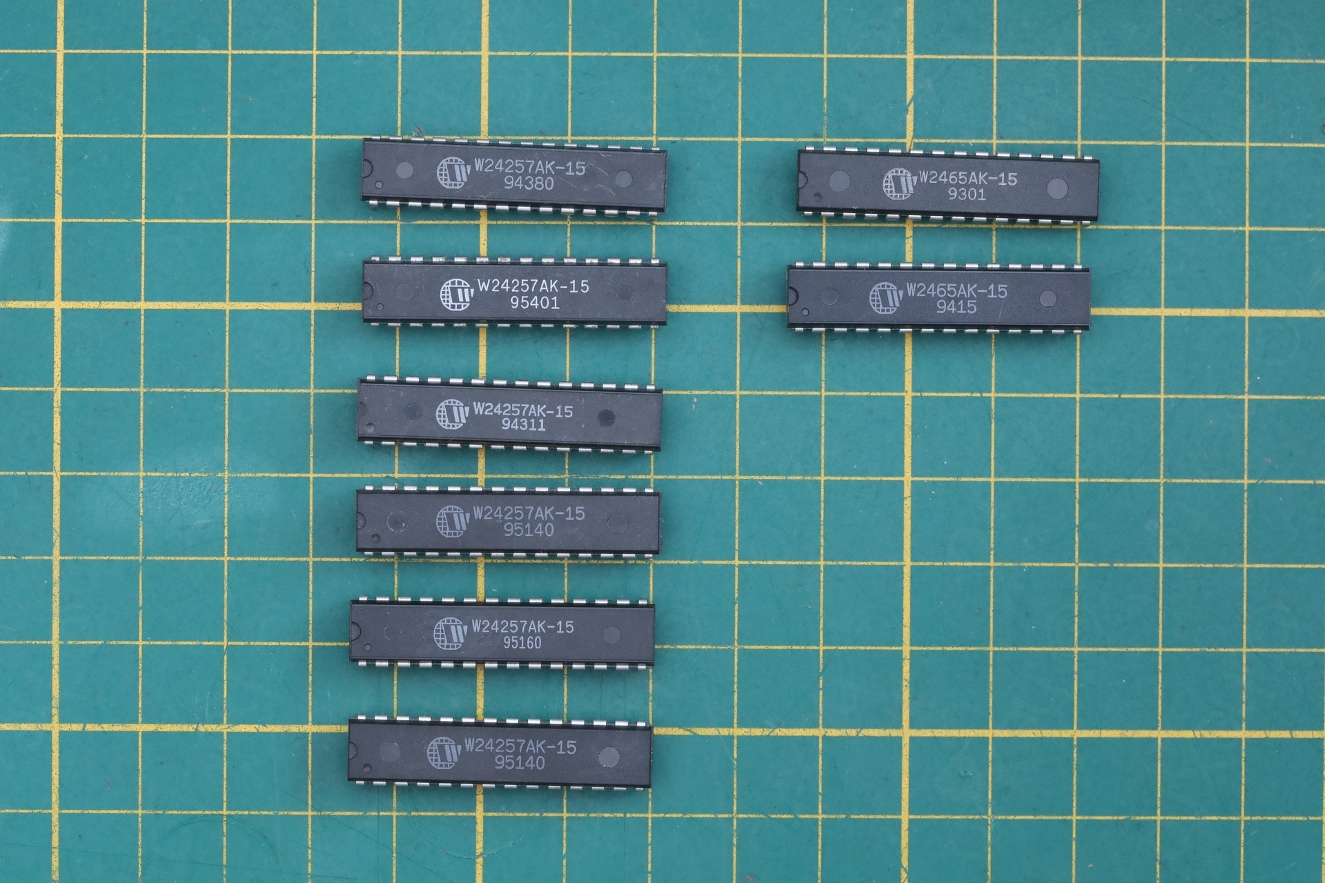
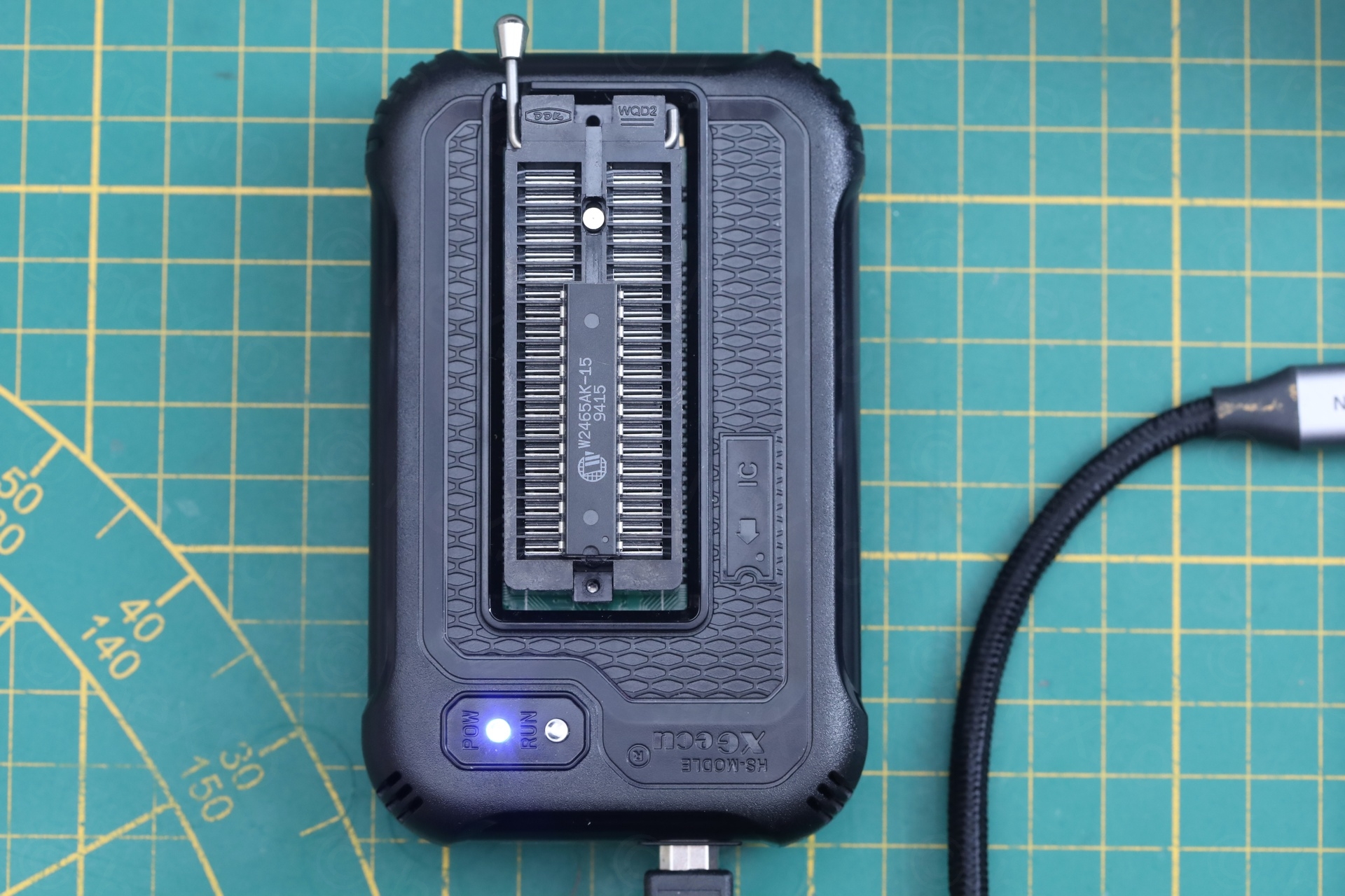
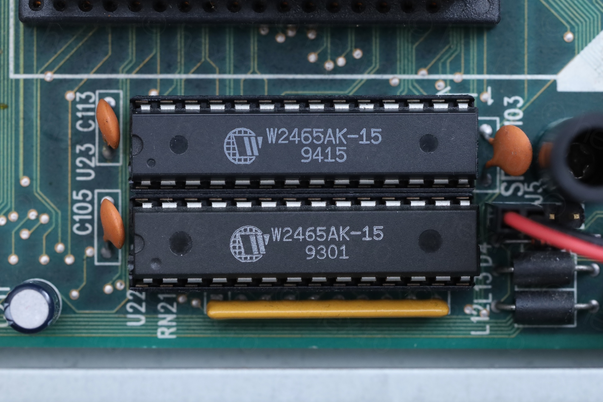
On this page: https://www.dosdays.co.uk/topics/review_opti386_486_mobo_1.php there is a small photo showing a TAG chip. Markings were a little blurry, but readable: W2465AK-15 for the TAG. Found a European seller that had both in stock, W2465AK-15 as well as W24257AK-15. Decided to bite the bullet and order 2 TAG chips and 6 cache memory chips. If all boards use these chips, maybe mine will work with them too ?! Fingers crossed.
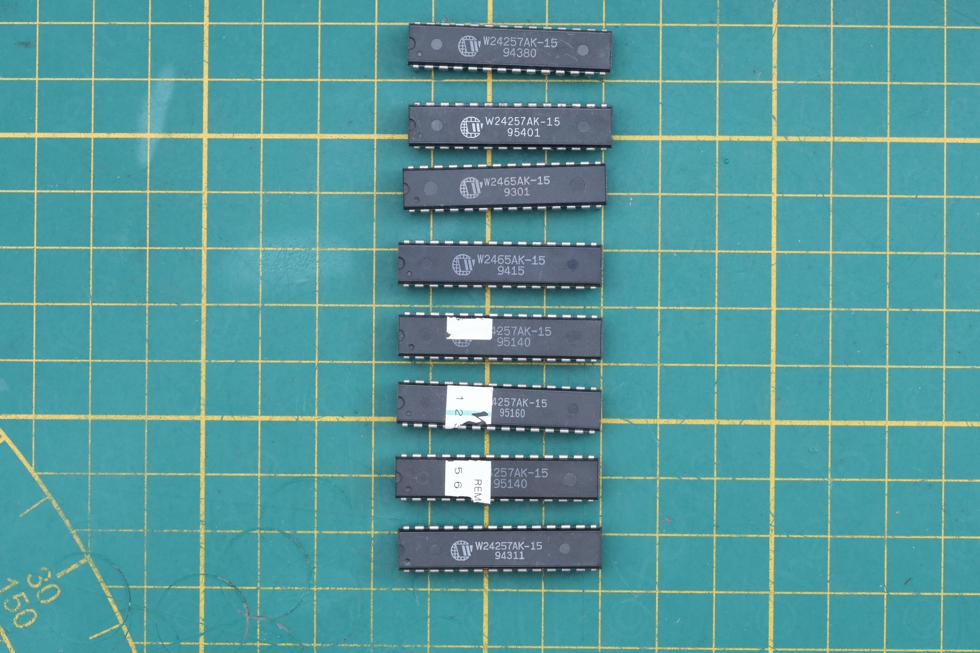
I was still convinced I need only 1 TAG chip (and was getting ready for some trial and error which socket will it be?). Ordered 2 for safe measure (what if 1 is bad ?).
I tested the chips with a programmer (all tested fine) and cleaned the sockets with contact cleaner. I tried all combinations – without TAG chip, a TAG chip in each socket (while other socket empty), and both TAG chips. It works only with both TAG chips installed.
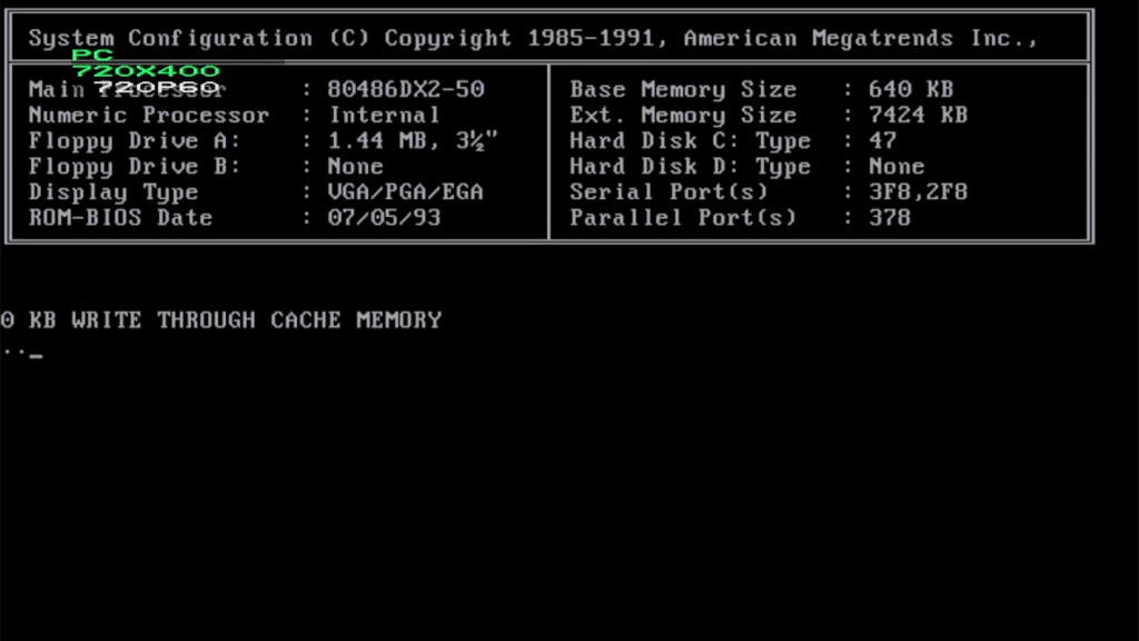
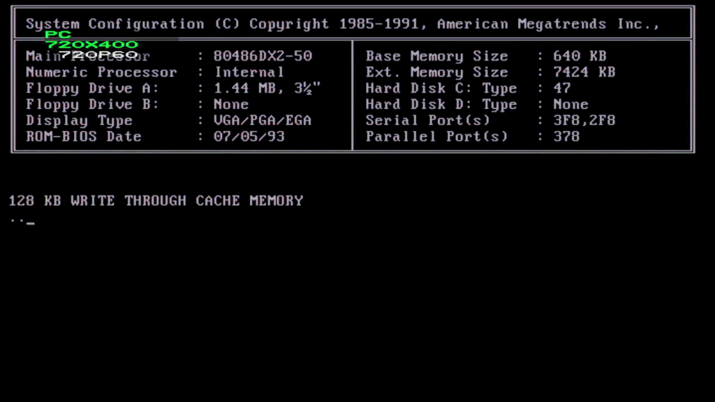
Results are below: it seems a bit faster (up to 128Kb) with the external cache enabled, and cache size is also reported by the BIOS:
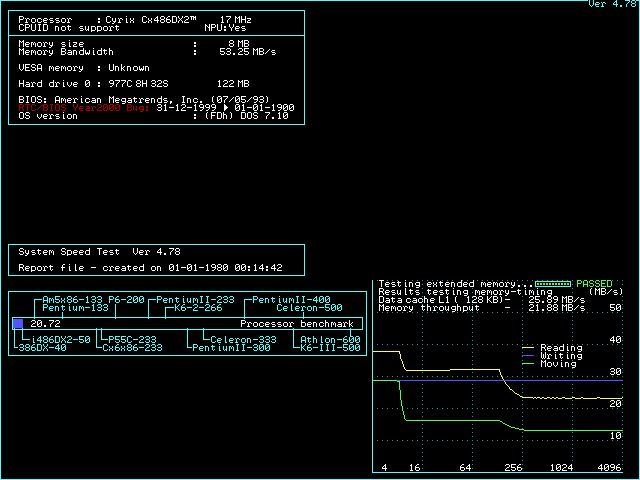
Benchmarks
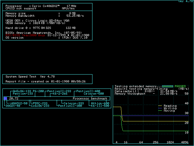
Curiosity pushed me further, to run DOS Benchmark Pack from Phil’s Computer Lab. Below a table with the test results, without cache chips and with them installed:
| Test program | Without Cache | With Cache |
| 3DBench 1.0 (Slower PCs) | 28.5 | 30.3 |
| 3DBench 1.0c (Faster PCs) | 28.5 | 29.8 |
| Chris’s 3D Benchmark | 29.7 (17.8 FPS) | 30.9 (18.5 FPS) |
| PC Player Benchmark | 7.3 | 7.9 |
| PC Player Benchmark 640×480 | 2.8 | 3.0 |
| Doom min. details (Slower PCs) | 1710 realticks (43.68 FPS) | 1516 realticks (49.27 FPS) |
| Doom max details (Faster PCs) | 4887 realticks (15.28 FPS) | 4617 realticks (16.18 FPS) |
| TOPBENCH 3.8 | 136 | 136 |
Is it worthy to populate the cache chips ? No … but I don’t regret trying it – at least I validated the choices I made for the ICs.
Unfortunately I found this post too late: 486 L2: Comparison between Write-Through & Write-Back (with and without dirty tag ram). It describes BIOS changes for cache. But PC was already packed, and now I wonder why I was in such a rush. Well, next time I’ll take it out, I’ll have a closer look, if I could squeeze more performance out of it.
I also had a look with the infrared camera: the TAG chips are the two above the CPU, and the 4 external cache chips are the top 4 on the left – they seem equally hot which is good, although the TAG chip closest to the CPU is a little cooler than the one closer to the edge of the motherboard:

Booting the PC
Before I end the blog-post, I figured I should mention that getting the OS to boot was tricky. The procedure to flash a Virtual Machine image ended up producing the message partition signature != 55AA. Procedure works on a more modern Slot 1 PC, but not on this one.
I had already identified the CHS settings, made sure the partition is set to active and trying to make it bootable with sys c: . Still the same error.
Solution was to make a real bootable floppy disk (using a USB Floppy adapter on my main PC), boot with the real FreeDos floppy, format and make C: bootable with the CF already installed. Then I could boot from the CF. The CF was still readable on the main PC – so I was able to copy the rest of FreeDOS data / folders on the main PC.
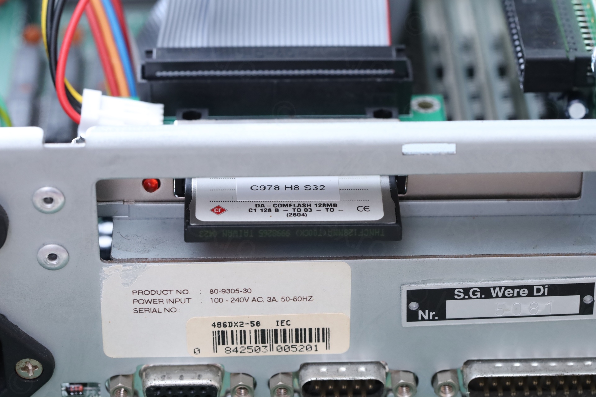
I put a small sticker on the CF card itself to not forget the CHS settings – and permanently installed a CF to IDE adapter onto the empty slot of the PC:
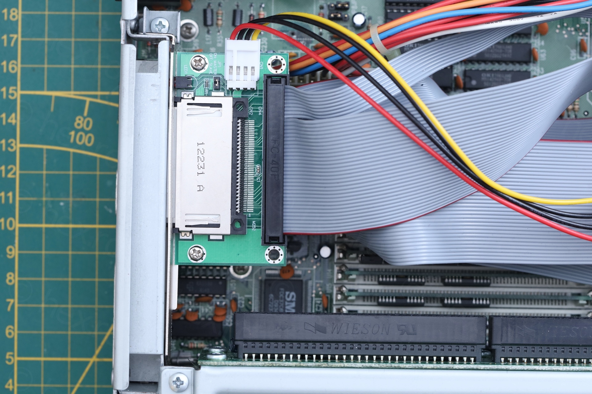
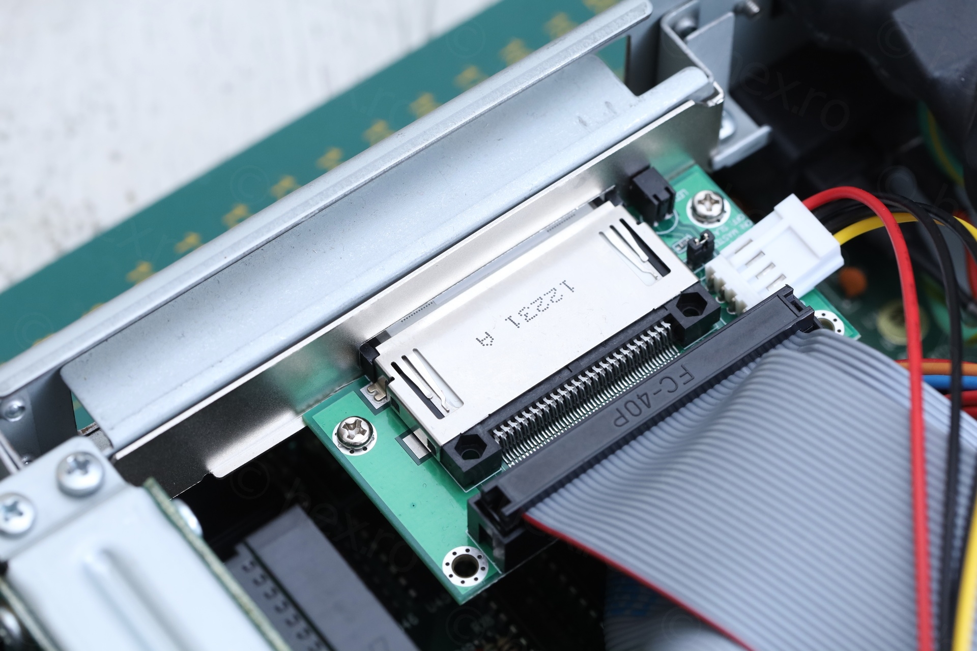
Seems that the small compact flash cards are very expensive, however, I found mine into a very cheap old photo camera at the flea market.
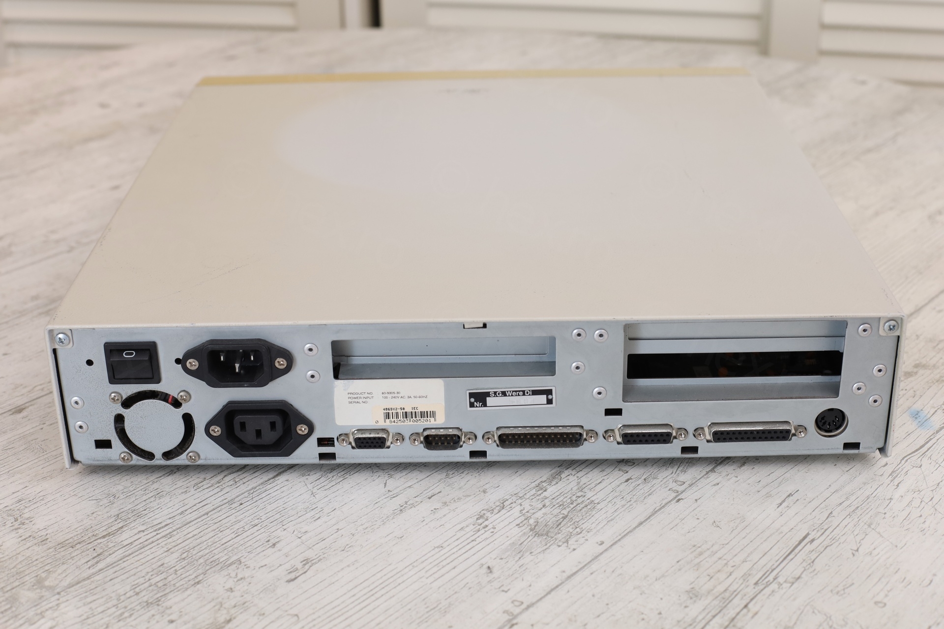
In conclusion, I can’t say I am overly enthusiastic about this PC. It is nice that it comes in the whole package: no need to worry about acquiring a case, a video card, floppy drive and building a PC from scrap. You can just plug it and it works. However, there is no sound card and only 3 ISA slots on the extension bracket, one of which is now taken by the CF adapter. But robust enough and it should last many more years now, having the corrosion removed.
Leave a Reply